Early microprocessors were very slow when operating with floating-point numbers. But in 1980, Intel introduced the 8087 floating-point coprocessor, performing floating-point operations up to 100 times faster. This was a huge benefit for IBM PC applications such as AutoCAD, spreadsheets, and flight simulators. The 8087 was so effective that today's computers still use a floating-point system based on the 8087.1
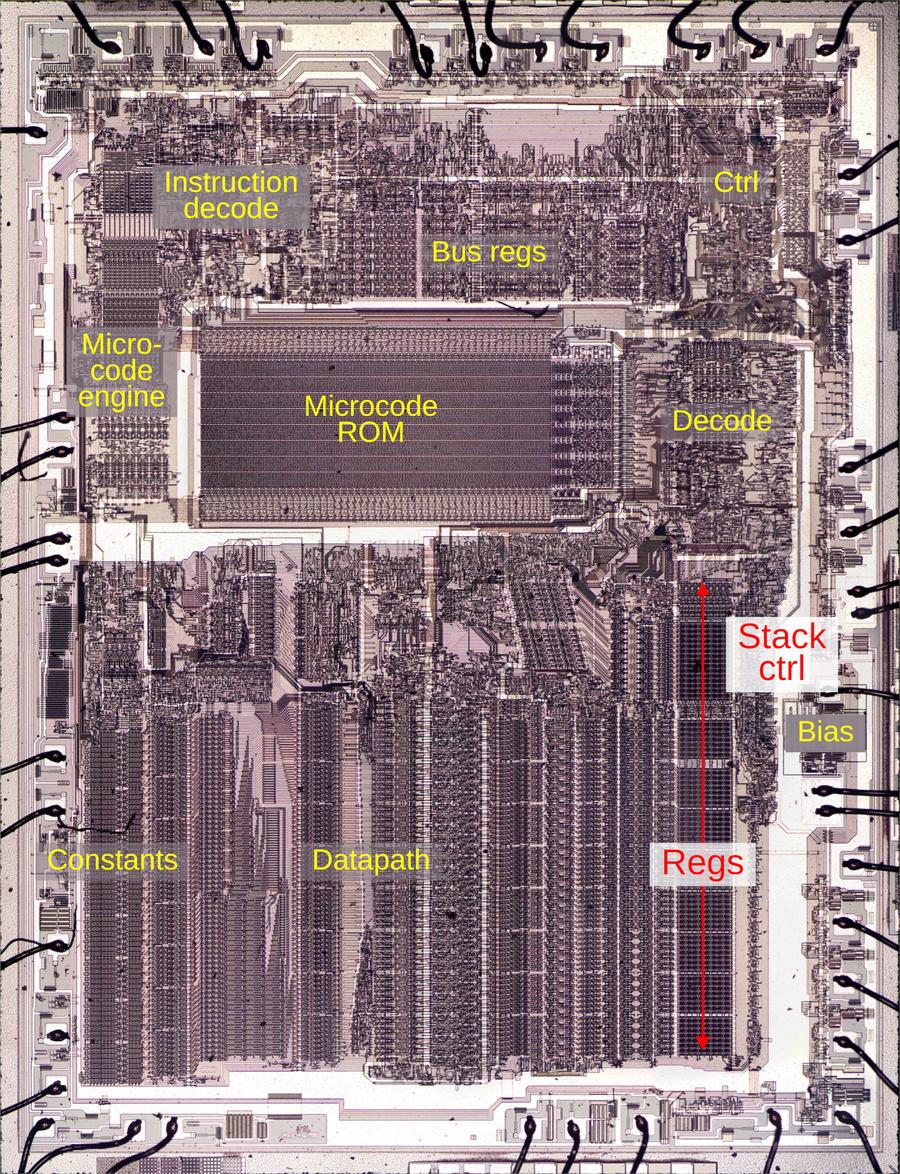
The 8087 was an extremely complex chip for its time, containing somewhere between 40,000 and 75,000 transistors, depending on the source.2 To explore how the 8087 works, I opened up a chip and took numerous photos of the silicon die with a microscope. Around the edges of the die, you can see the hair-thin bond wires that connect the chip to its 40 external pins. The complex patterns on the die are formed by its metal wiring, as well as the polysilicon and silicon underneath. The bottom half of the chip is the "datapath", the circuitry that performs calculations on 80-bit floating point values. At the left of the datapath, a constant ROM holds important constants such as π. At the right are the eight registers that form the stack, along with the stack control circuitry.

Die of the Intel 8087 floating point unit chip, with main functional blocks labeled. The die is 5mm×6mm. Click for a larger image.
The chip's instructions are defined by the large microcode ROM in the middle. This ROM is very unusual; it is semi-analog, storing two bits per transistor by using four transistor sizes. To execute a floating-point instruction, the 8087 decodes the instruction and the microcode engine starts executing the appropriate micro-instructions from the microcode ROM. The decode circuitry to the right of the ROM generates the appropriate control signals from each micro-instruction. The bus registers and control circuitry handle interactions with the main 8086 processor and the rest of the system. Finally, the bias generator uses a charge pump to create a negative voltage to bias the chip's substrate, the underlying silicon.
The stack registers and control circuitry (in red above) are the subject of this blog post. Unlike most processors, the 8087 organizes its registers in a stack, with instructions operating on the top of the stack. For instance, the square root instruction replaces the value on the top of the stack with its square root. You can also access a register relative to the top of the stack, for instance, adding the top value to the value two positions down from the top. The stack-based architecture was intended to improve the instruction set, simplify compiler design, and make function calls more efficient, although it didn't work as well as hoped.

The stack on the 8087. From The 8087 Primer, page 60.
The diagram above shows how the stack operates. The stack consists of eight registers, with the Stack Top (ST) indicating the current top of the stack. To push a floating-point value onto the stack, the Stack Top is decremented and then the value is stored in the new top register. A pop is performed by copying the value from the stack top and then incrementing the Stack Top. In comparison, most processors specify registers directly, so register 2 is always the same register.
The registers
The stack registers occupy a substantial area on the die of the 8087 because floating-point numbers take many bits. A floating-point number consists of a fractional part (sometimes called the mantissa or significand), along with the exponent part; the exponent allows floating-point numbers to cover a range from extremely small to extremely large. In the 8087, floating-point numbers are 80 bits: 64 bits of significand, 15 bits of exponent, and a sign bit. An 80-bit register was very large in the era of 8-bit or 16-bit computers; the eight registers in the 8087 would be equivalent to 40 registers in the 8086 processor.

The registers in the 8087 form an 8×80 grid of cells. The close-up shows an 8×8 block. I removed the metal layer with acid to reveal the underlying silicon circuitry.
The registers store each bit in a static RAM cell. Each cell has two inverters connected in a loop. This circuit forms a stable feedback loop, with one inverter on and one inverter off. Depending on which inverter is on, the circuit stores a 0 or a 1. To write a new value into the circuit, one of the lines is pulled low, flipping the loop into the desired state. The trick is that each inverter uses a very weak transistor to pull the output high, so its output is easily overpowered to change the state.

Two inverters in a loop can store a 0 or a 1.
These inverter pairs are arranged in an 8 × 80 grid that implements eight words of 80 bits. Each of the 80 rows has two bitlines that provide access to a bit. The bitlines provide both read and write access to a bit; the pair of bitlines allows either inverter to be pulled low to store the desired bit value. Eight vertical wordlines enable access to one word, one column of 80 bits. Each wordline turns on 160 pass transistors, connecting the bitlines to the inverters in the selected column. Thus, when a wordline is enabled, the bitlines can be used to read or write that word.
Although the chip looks two-dimensional, it actually consists of multiple layers. The bottom layer is silicon. The pinkish regions below are where the silicon has been "doped" to change its electrical properties, making it an active part of the circuit. The doped silicon forms a grid of horizontal and vertical wiring, with larger doped regions in the middle. On top of the silicon, polysilicon wiring provides two functions. First, it provides a layer of wiring to connect the circuit. But more importantly, when polysilicon crosses doped silicon, it forms a transistor. The polysilicon provides the gate, turning the transistor on and off. In this photo, the polysilicon is barely visible, so I've highlighted part of it in red. Finally, horizontal metal wires provide a third layer of interconnecting wiring. Normally, the metal hides the underlying circuitry, so I removed the metal with acid for this photo. I've drawn blue lines to represent the metal layer. Contacts provide connections between the various layers.

A close-up of a storage cell in the registers. The metal layer and most of the polysilicon have been removed to show the underlying silicon.
The layers combine to form the inverters and selection transistors of a memory cell, indicated with the dotted line below. There are six transistors (yellow), where polysilicon crosses doped silicon. Each inverter has a transistor that pulls the output low and a weak transistor to pull the output high. When the word line (vertical polysilicon) is active, it connects the selected inverters to the bit lines (horizontal metal) through the two selection transistors. This allows the bit to be read or written.

The function of the circuitry in a storage cell.
Each register has two tag bits associated with it, an unusual form of metadata to indicate if the register is empty, contains zero, contains a valid value, or contains a special value such as infinity. The tag bits are used to optimize performance internally and are mostly irrelevant to the programmer. As well as being accessed with a register, the tag bits can be accessed in parallel as a 16-bit "Tag Word". This allows the tags to be saved or loaded as part of the 8087's state, for instance, during interrupt handling.
The decoder
The decoder circuit, wedged into the middle of the register file, selects one of the registers. A register is specified internally with a 3-bit value. The decoder circuit energizes one of the eight register select lines based on this value.
The decoder circuitry is straightforward: it has eight 3-input NOR gates to match one of the eight bit patterns. The select line is then powered through a high-current driver that uses large transistors. (In the photo below, you can compare the large serpentine driver transistors to the small transistors in a bit cell.)

The decoder circuitry has eight similar blocks to drive the eight select lines.
The decoder has an interesting electrical optimization. As shown earlier, the register select lines are eight polysilicon lines running vertically, the length of the register file. Unfortunately, polysilicon has fairly high resistance, better than silicon but much worse than metal. The problem is that the resistance of a long polysilicon line will slow down the system. That is, the capacitance of transistor gates in combination with high resistance causes an RC (resistive-capacitive) delay in the signal.
The solution is that the register select lines also run in the metal layer, a second set of lines immediately to the right of the register file. These lines branch off from the register file about 1/3 of the way down, run to the bottom, and then connect back to the polysilicon select lines at the bottom. This reduces the maximum resistance through a select line, increasing the speed.

A diagram showing how 8 metal lines run parallel to the main select lines. The register file is much taller than shown; the middle has been removed to make the diagram fit.
The stack control circuitry
A stack needs more control circuitry than a regular register file, since the circuitry must keep track of the position of the top of the stack.3 The control circuitry increments and decrements the top of stack (TOS) pointer as values are pushed or popped (purple).4 Moreover, an 8087 instruction can access a register based on its offset, for instance the third register from the top. To support this, the control circuitry can temporarily add an offset to the top of stack position (green). A multiplexer (red) selects either the top of stack or the adder output, and feeds it to the decoder (blue), which selects one of the eight stack registers in the register file (yellow), as described earlier.

The physical implementation of the stack circuitry is shown below. The logic at the top selects the stack operation based on the 16-bit micro-instruction.5 Below that are the three latches that hold the top of stack value. (The large white squares look important, but they are simply "jumpers" from the ground line to the circuitry, passing under metal wires.)

The stack control circuitry. The blue regions on the right are oxide residue that remained when I dissolved the metal rail for the 5V power.
The three-bit adder is at the bottom, along with the multiplexer. You might expect the adder to use a simple "full adder" circuit. Instead, it is a faster carry-lookahead adder. I won't go into details here, but the summary is that at each bit position, an AND gate produces a Carry Generate signal while an XOR gate produces a Carry Propagate signal. Logic gates combine these signals to produce the output bits in parallel, avoiding the slowdown of the carry rippling through the bits.
The incrementer/decrementer uses a completely different approach. Each of the three bits uses a toggle flip-flop. A few logic gates determine if each bit should be toggled or should keep its previous value. For instance, when incrementing, the top bit is toggled if the lower bits are 11 (e.g. incrementing from 011 to 100). For decrementing, the top bit is toggled if the lower bits are 00 (e.g. 100 to 011). Simpler logic determines if the middle bit should be toggled. The bottom bit is easier, toggling every time whether incrementing or decrementing.
The schematic below shows the circuitry for one bit of the stack. Each bit is implemented with a moderately complicated flip-flop that can be cleared, loaded with a value, or toggled, based on control signals from the microcode. The flip-flop is constructed from two set-reset (SR) latches. Note that the flip-flop outputs are crossed when fed back to the input, providing the inversion for the toggle action. At the right, the multiplexer selects either the register value or the sum from the adder (not shown), generating the signals to the decoder.

Schematic of one bit of the stack.
Drawbacks of the stack approach
According to the designers of the 8087,7 the main motivation for using a stack rather than a flat register set was that instructions didn't have enough bits to address multiple register operands. In addition, a stack has "advantages over general registers for expression parsing and nested function calls." That is, a stack works well for a mathematical expression since sub-expressions can be evaluated on the top of the stack. And for function calls, you avoid the cost of saving registers to memory, since the subroutine can use the stack without disturbing the values underneath. At least that was the idea.
The main problem is "stack overflow". The 8087's stack has eight entries, so if you push a ninth value onto the stack, the stack will overflow. Specifically, the top-of-stack pointer will wrap around, obliterating the bottom value on the stack. The 8087 is designed to detect a stack overflow using the register tags: pushing a value to a non-empty register triggers an invalid operation exception.6
The designers expected that stack overflow would be rare and could be handled by the operating system (or library code). After detecting a stack overflow, the software should dump the existing stack to memory to provide the illusion of an infinite stack. Unfortunately, bad design decisions made it difficult "both technically and commercially" to handle stack overflow.
One of the 8087's designers (Kahan) attributes the 8087's stack problems to the time difference between California, where the designers lived, and Israel, where the 8087 was implemented. Due to a lack of communication, each team thought the other was implementing the overflow software. It wasn't until the 8087 was in production that they realized that "it might not be possible to handle 8087 stack underflow/overflow in a reasonable way. It's not impossible, just impossible to do it in a reasonable way."
As a result, the stack was largely a problem rather than a solution.
Most 8087 software saved the full stack to memory before performing
a function call, creating more memory traffic.
Moreover, compilers turned out to work better with regular registers than a stack,
so compiler writers awkwardly used the stack to emulate regular registers.
The GCC compiler reportedly needs 3000 lines of extra code to support the x87 stack.
In the 1990s, Intel introduced a new floating-point system called SSE, followed by AVX in 2011. These systems use regular (non-stack) registers and provide parallel operations for higher performance, making the 8087's stack instructions largely obsolete.
The success of the 8087
At the start, Intel was unenthusiastic about producing the 8087, viewing it as unlikely to be a success. John Palmar, a principal architect of the chip, had little success convincing skeptical Intel management that the market for the 8087 was enormous. Eventually, he said, "I'll tell you what. I'll relinquish my salary, provided you'll write down your number of how many you expect to sell, then give me a dollar for every one you sell beyond that."7 Intel didn't agree to the deal—which would have made a fortune for Palmer—but they reluctantly agreed to produce the chip.
Intel's Santa Clara engineers shunned the 8087, considering it unlikely to work: the 8087 would be two to three times more complex than the 8086, with a die so large that a wafer might not have a single working die. Instead, Rafi Nave, at Intel's Israel site, took on the risky project: “Listen, everybody knows it's not going to work, so if it won't work, I would just fulfill their expectations or their assessment. If, by chance, it works, okay, then we'll gain tremendous respect and tremendous breakthrough on our abilities.”
A small team of seven engineers developed the 8087 in Israel. They designed the chip on Mylar sheets: a millimeter on Mylar represented a micron on the physical chip. The drawings were then digitized on a Calma system by clicking on each polygon to create the layout. When the chip was moved into production, the yield was very low but better than feared: two working dies per four-inch wafer.
The 8087 ended up being a large success, said to have been Intel's most profitable product line at times. The success of the 8087 (along with the 8088) cemented the reputation of Intel Israel, which eventually became Israel's largest tech employer. The benefits of floating-point hardware proved to be so great that Intel integrated the floating-point unit into later processors starting with the 80486 (1989). Nowadays, most modern computers, from cellphones to mainframes, provide floating point based on the 8087, so I consider the 8087 one of the most influential chips ever created.
For more, follow me on Bluesky (@righto.com), Mastodon (@[email protected]), or RSS. I wrote some articles about the 8087 a few years ago, including the die, the ROM, the bit shifter, and the constants, so you may have seen some of this material before.