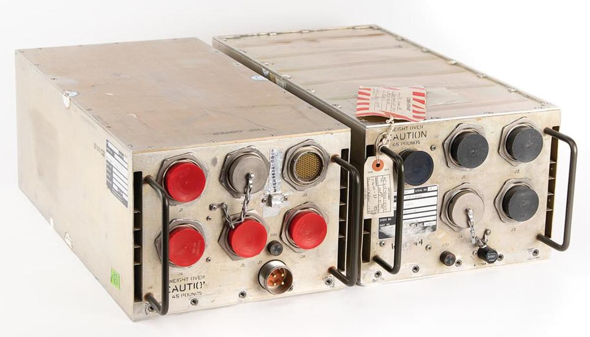
The Space Shuttle's five1 general-purpose computers played a critical role in each flight: controlling the engines, monitoring thousands of sensors, displaying data to the astronauts, and navigating the Shuttle. Each computer consisted of two 60-pound aluminum-alloy boxes: the box on the right is the CPU, a 32-bit processor that executed 420,000 instructions per second. These computers were designed before microprocessors became popular, so the processor was built from multiple boards crammed with simple chips and they used magnetic core memory rather than DRAM chips.
. Photo courtesy of RR Auction.")
The box on the left is the I/O Processor (IOP): the link between the CPU and the rest of the Shuttle. It implemented the input/output capabilities for the computer, primarily 24 high-speed networks that connected the computer to the Shuttle's systems and sensors. But the IOP wasn't just a peripheral; it was a separate programmable computer, more complicated than the main CPU. The IOP had an unusual architecture: it was one of the first multi-threaded computers, implementing 25 virtual processors (with two completely different instruction sets) that ran on one physical processor.
I obtained two circuit cards from the I/O Processor,2 each a 9"×3" rectangle packed with tiny chips and other components. In IBM lingo, each card is called a "page" (remember this term). The top page is a network interface, providing four network connections, each handling 1 million bits per second. (The IOP contained six of these cards for its 24 network connections.) The bottom page held the microcode for the IOP's processors, the low-level code that defined each instruction. The rows of white-and-gold chips stored the microcode's bits in tiny metal fuses, programmed by blowing a fuse for each 1 bit. In this article, I'll explain how the I/O Processor worked, and the roles of these two pages.

Two pages from the Space Shuttle I/O Processor: the "MIA" interface page and the PROM page.
The MIA interface page
The Space Shuttle had 28 data bus networks that linked the computers to the rest of the Shuttle, with each computer attached to 24 of the networks.3 The large number of networks provided both high performance and reliability, with at least two networks between a computer and any Shuttle system. Eight networks were assigned to flight-critical systems, with each CRT display and engine controller connected to four networks for redundancy.
The page below is one of the six network interface pages in the I/O Processor. Space Shuttle engineers loved acronyms, so this page has the cryptic name MIA for "Multiplexer Interface Adapter". (Many of the networks were connected to boxes called Multiplexer/Demultiplexers, which provided the link between the network and the diverse analog and digital components of the Space Shuttle.5) The MIA interface page is tightly packed with integrated circuits and other components. The page holds two printed-circuit boards, one on each side of the page. The boards on both sides are almost identical,4 as you can see by comparing the photo above and the photo below. (Main difference: the connector switches sides.)
.
The page has extensive rework; thin brown \"bodge\" wires snake around the page to
repair errors or implement updates.")
The network interface page, called the MIA (Multiplex Interface Adapter). The page has extensive rework; thin brown "bodge" wires snake around the page to repair errors or implement updates.
Each board implements two network interfaces, so the page supports four networks. Each network transmits data across a pair of wires, twisted together and shielded, rather than a coaxial cable. Although the network transmits digital data, the signals transmitted across the network are physical voltages that will weaken with distance and will have distortion and noise. Thus, the interface page must convert these analog signals back to 0's and 1's.
The right half of the board holds the analog circuitry. It is dominated by a large golden module labeled "IBM", with 46 pins. This is a hybrid module, consisting of tiny components such as transistor dies, resistors, capacitors, and potentially IC dies, connected by bond wires thinner than a hair. It's not quite an integrated circuit, but a collection of individual components mounted on a ceramic wafer. Hybrid modules were popular for aerospace applications, since a board of analog components could be shrunk down to a single (expensive) module. This module contains the analog circuitry for two I/O ports: the drivers to transmit network signals along with the amplifiers and comparators to receive signals.
Various discrete components are mounted next to the hybrid module: resistors, glass capacitors6, inductors, and small square transformers. The transformers provide the coupling between the interface board and the network. As with Ethernet, transformers provide isolation between the computer and the network, filter electromagnetic interference, and match impedances, all important for reliability.7

A key part of the Shuttle's networking dates back to the 1940s. In 1946, Frederic Williams became head of the Electrical Engineering department at the University of Manchester. By 1949, his team had created the groundbreaking Manchester Mark 1 computer. Along the way, they invented the stored-program computer, the Williams tube—the best form of computer memory before magnetic core—and the Manchester Carry Chain, still used for addition in modern processors.
But the relevant invention is the patented Manchester encoding, a way of encoding a sequence of 0's and 1's for storage or transmission. In the Manchester encoding, each 0 bit is replaced by a "low-high" sequence and each 1 bit is replaced by a "high-low" sequence, as shown below. This idea may seem trivial, but it is used in everything from floppy disks and remote controls to Ethernet and RFID tags, earning it recognition as an IEEE Milestone.

The obvious approach—sending binary data unencoded—has two problems. First, in a long string of 0's or 1's, it is hard to tell how many bits were sent: "Was that six bits or only five?" Second, such a sequence is unbalanced, so it has a "DC component". This DC component causes problems if the signal is stored on a magnetic medium or transmitted through a transformer. The Manchester encoding solves both these problems. Since every encoded bit has a transition in the middle, it is straightforward to separate the bits. Moreover, the encoding ensures that 0's and 1's occur in equal numbers, so there is no DC component.
Because of these advantages, the Manchester encoding was selected for the data bus networks in the Space Shuttle.8 One of the key functions9 of the IOP's network interfaces is to convert between serial bits and the Manchester encoding. The digital circuitry for the interface is fairly complicated, but most of the logic is in the four large golden integrated circuits. These are custom Motorola integrated circuits: a transmit chip and a receive chip for each network port. On the transmit side, the chip converts binary data into the Manchester-encoded signals for the network. The circuitry also inserts a sync signal at the beginning of each word and adds parity. The receive chip reverses this process: detecting sync, decoding the Manchester signals, verifying the parity, and reporting any errors.
The smaller black chips are simple TTL chips, mostly shift registers. (Transistor-Transistor Logic was very popular in the 1970s, providing fast, reliable circuits.) There are twelve 4-bit shift register chips and sixteen 8-bit shift registers.10 The Shuttle's networks sent 24-bit words across the network: combining six 4-bit shift register chips produces a 24-bit shift register, which converted these 24-bit words to serial data and vice versa. The remaining chips are simple logic gates, flip-flops, buffers, and four-bit counters.
The physical structure of a page
Around 1967, IBM introduced a line of computers for avionics, called System/4 Pi.11 These systems were constructed from pages:12 two circuit boards sandwiching a metal layer that provided convection cooling. Flat-pack integrated circuits, smaller than a fingernail, were mounted in rows13 on each circuit board, about 78 ICs on a board. The printed-circuit boards were advanced for the time, with six layers of wiring. Two jack screws at the top tightly secured the page into the system. Two 98-pin connectors connected the page to the backplane. The photo below shows a typical 4 Pi page (top), with its rows of chips.

A comparison of a standard IBM 4 Pi page with the IOP page. 4 Pi page courtesy of Eric Schlaepfer. The 4 Pi page was in a bag labeled "FSD AWACS tester?" suggesting that it was a tester from IBM's Federal Systems Division for the E-3C Airborne Warning and Control System aircraft, which used an IBM 4 Pi computer.
An I/O processor page (above, bottom) is almost identical to a standard 4 Pi page except that it is one inch wider (9" instead of 8"), and has a 120-pin connector or two instead of 98-pin connectors.14 One inch may not seem like much, but a 9-inch page fits 100 ICs rather than 78, a significant increase. I'm surprised that IBM changed from the standard size, but I suspect that the designers couldn't fit the IOP into the available space with standard pages, forcing the change. Likewise, the multiple I/O ports may have required more connections than the smaller connectors could support.
A page has circuit boards on either side, separated by a metal plate. To allow signals to flow between the boards, a special connector is attached to the top of the page to link the two boards. This connector not only provides feed-through connections between the boards, but also provides test points, so signals can be probed while the boards are mounted in the case. The photo below shows a close-up of the feed-through connector. It has three rows of test points. The first row (red) is connected to the top board. The middle row (orange) is connected to both boards and provides the feed-throughs. The bottom row (blue) is connected to the bottom board. The upper arrows show where the connector is soldered to the board.

The test point connector on the MIA page.
The diagram below shows the construction of the I/O Processor, with rows of pages plugged into the backplane.15 Note the 128-pin MIA I/O connector on the front of the IOP; this connects the 24 data buses (along with other signals) to other parts of the Shuttle. The arrows show how cooling air flowed through the sides of the IOP. The air did not flow over the pages. Instead, heat was transmitted by convection through the metal plate inside each page, flowing to heat exchangers in the sides of the case. The CPU and the IOP both contained magnetic core memory (labeled "Storage Page" below); even though the memory is split between the boxes, it is treated as a unified shared memory, so programs for the CPU and the IOP can reside in memory in either physical box.

The IOP's architecture and the PROM page
The high-performance design of the I/O Processor was developed by Peter Kogge, an expert in parallel processing architectures. At the time, he was working at IBM's Federal Systems Division, where the Space Shuttle computer was developed. Kogge, now a professor at the University of Notre Dame, is also known for the Kogge-Stone adder, a fast circuit used in processors such as the Pentium. The I/O Processor has a very unusual architecture: although it had one physical processor, it ran 25 virtual processors with two completely different instruction sets. The virtual processors took turns, running for just one clock cycle and then letting the next processor run. The motivation behind this was to ensure that each network port got a predictable and guaranteed portion of the processor, so even if one network port was overloaded, it wouldn't affect the others. This approach, called a barrel processor16, was first used in the CDC 6600 supercomputer, the world's fastest computer from 1964 to 1969.
The I/O Processor has two types of (virtual) processors, which of course have cryptic acronyms: BCE and MSC. Each of the 24 network ports has a BCE, a Bus Control Element, which runs a small program to move data words between the network port and memory. An MSC (Master Sequence Controller) is the executive, running programs to manage the BCEs. The BCE and MSC processors run code that is stored in the computer's core memory. The instruction sets of the MSC and the BCE are completely different from each other and from the instruction set of the main CPU (which is derived from IBM's System/360 mainframes). The (executive) MSC is a 32-bit processor with the standard instructions of a normal processor—addition, logic, branches, and so forth—as well as specialized operations to configure and start BCEs.17 The instruction set of a low-level BCE is much smaller and much stranger, lacking all the basic instructions such as arithmetic and conditional branches. the instructions you'd expect from a processor. Instead, a BCE has I/O instructions such as Transmit Data, Receive Data, Load Timeout Register, Store Status, and Wait. In typical use, the CPU directs the MSC to run a program, the MSC configures the BCEs to execute a program, and the BCEs send and receive data as specified. When the BSE's operation is done, the MSC interrupts the CPU, which processes the data. Thus, the CPU can focus on the high-level algorithms without wasting cycles on network operations.
How do the MSC and BCE processors all run on one physical processor, when they have completely different instruction sets? The trick is microcode: each MSC and BCE instruction was implemented in microcode, through a sequence of 72-bit micro-instructions.18 A simple instruction might take five micro-instructions, while a complex instruction might require 60 micro-instructions. Each micro-instruction directed the action of the IOP's physical processor for one step of the MSC or BCE instruction. After each micro-instruction, the physical processor switched to the micro-instruction for the next virtual processor. The architecture of the physical processor was completely different from the MSC or the BCE: three 16-bit data paths and two ALUs (Arithmetic/Logic Units) that can operate in parallel. The physical processor had a separate register set, including a micro-instruction address register, for each virtual processor, to keep track of the state of each virtual processor.

The PROM page holds the majority of the microcode for the I/O Processor. Although three chips are mounted sideways to avoid wasting space, there is even more wasted space at the left.
The IOP's micro-instructions were stored in the PROM page above. In the photo above, the white chips with gold lids are fusible-link PROM (Programmable Read-Only Memory) chips.19 These unusual chips contain a tiny fuse for each bit. If the fuse is intact, the corresponding bit is a 0, while a burnt-out fuse represents a 1 bit. The chip is programmed by applying 17-volt pulses to destroy fuses one by one, literally burning the PROM. (I discussed fusible PROM chips earlier.)
Each PROM chip holds 512 words of 4 bits, so in total, this page held 1024 72-bit micro-instructions; the remaining 512 micro-instructions were in another page.20 The chips are hand-labeled with numbers, since each chip has unique programming and must be installed in the correct location. With 36 chips, you'd expect the chips to be numbered from 1 to 36. Curiously, although many of the chips are sequentially numbered, others have numbers ranging from 55 to 74 in no obvious pattern.21
Physically, the PROM page is unusual in several ways. Instead of flat-pack integrated circuits, it uses DIP (Dual-Inline Package) ICs, larger integrated circuits with two rows of vertical pins that go through the circuit board. Since this page only has one circuit board, it doesn't have the test-point feed-throughs at the top. It still has the central metal plate, but the integrated circuits sit on top of the metal plate, while the circuit board is underneath—the plate has gaps for the pins. Between the rows of chips, the central plate is the full thickness of the board.

A close-up of the PROM page, showing how the chips are mounted. The black chips are much thicker than the white chips.
Presumably, the fusible-link PROM chips were only available in DIP packages, rather than flat-packs. These DIP packages take up much more space than the regular flat-pack integrated circuits; this page has about a quarter the density of a regular page.22
Conclusions
The Space Shuttle's CPU and IOP were advanced when they were designed, but they rapidly became obsolete. IBM redesigned the computer, combining both the CPU and IOP into a single box called the AP-101S, which first flew in 1991 (details). The improved computer was much faster and had more memory. Moreover, combining two boxes into one saved about 300 pounds in total. The photo below shows three of the updated AP-101S computers mounted in the Shuttle's avionics bays. (The wall hides the fourth computer, and the fifth is behind the camera.) These same positions are where the I/O Processors were mounted previously, with the CPUs installed in the empty spaces to the left.

Despite the critical role of the I/O Processor in the Space Shuttle, it doesn't get the attention given to the CPU. For instance, although NASA documents describe the architecture of the IOP in detail, I couldn't find any photos of its pages.23 I hope that this article has convinced you that the architecture and the physical construction of the IOP make it an interesting system.
For updates, follow me on Bluesky (@righto.com), Mastodon (@[email protected]), or RSS. Thanks to Richard for supplying the boards. Thanks to Mike Stewart for documents on the IOP. Thanks to Richard Katz, Robert Pearlman of collectSPACE, and RR Auction for photos.
AI statement: I didn't use AI to write this article; the em-dashes are natural (details).