The high-bandwidth flash (HBF) market could be bigger than high-bandwidth memory (HBM) in 12 years’ time according to the leading HBF evangelist, Professor Kim Jung-ho of the School of Electrical Engineering at the Korea Advanced Institute of Science and Technology (KAIST).
He revealed this and more on a talk about HBF technology at a “Materials, Components, and Equipment (So-Bu-Jang) Future Forum” held in Seoul, S Korea, on January 16. HBF progress is accelerating. As reported in the Sisa Journal, he said: “Samsung Electronics and SanDisk plan to integrate HBF into products from Nvidia, AMD, and Google by late next year or early 2028.”
He conceives of High-Bandwidth Memory (HBM) acting as a very fast data cache layer for GPU accelerators with a tier of HBF feeding that, and slower but much higher capacity networked SSD storage feeding the HBF tier.
Nvidia has announced an Inference Context Memory Storage Platform (ICMSP) where its Dynamo and NIXL software provides a managed memory space for AI Inferencing tokens stored in a KV cache that covers HBM and BlueField-4-connected SSDs. Intuitively the same 2-tier software could be extended to cover a 3-tier HBM to HBF to BlueField-4-connected SSDs arrangement.
Networked, external storage would then connect to the BlueField-4 SSD tier and have a clear path to the GPUs with no diversion though a host X86 processor and its DRAM.
The KAIST professor discussed an HBF unit having a capacity of 512 GB and a 1.638 TBps bandwidth. This capacity compares to a 2Tb (250 GB) 3D NAND die, such as one built by SK hynix using its 321-layer, triple-string 3D NAND. We would only need to stack two of these to create a 512 GB capacity HBF chip.
Such a 2-layer chip would contain 642 layers of 3D NAND in total, in six component strings, and would need to be fabricated such that the upper layers did not warp the lower ones.
SK hynix is developing AIN B NAND products using HBF technology. A conceptual diagram (above) shows four NAND core layers stacked above a Base/Logic die which is attached to an interposer unit connecting this entire stack to a host processor.
HBF diagrams from both SK hynix and Sandisk show the upper layers in an HBM stack connecting by Through Silicon Vias (TSVs) or plugs, vertical electronic connections, through the lower layers to a Base/Logic die.
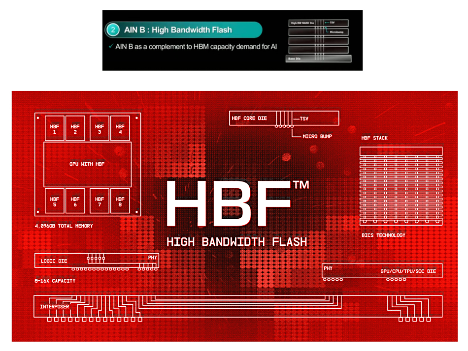
That means the lower stack has to be fabricated with TSVs or plugs passing through it, and cannot be a standard or normal 3D NAND die, with no such connections passing through it. The die area has to be larger to accommodate the TSVs/plugs. Adding additional 3D NAND die stacks to an HBF unit would mean even more TSVs or plugs would have to be added to the lower stacks, increasing their size further.
Jung-ho said HBF could have a broader adoption in the HBM6 era, when the HBM will likely insist of multiple interconnected separate stacks instead of a single stack. He is quoted as suggesting that the size of the HBF market will be bigger than HBM by 2038.
SK hynix is expected to reveal a prototype version of HBF later this month. It and Sandisk are promoting HBF standardization and, DigiTimes reports, Samsung has joined in, with Memorandums of Understanding (MOUs) and a consortium formed. Product is expected as early as 2027.
Kioxia prototyped a 5TB HBF module in August last year. It used a PCIe gen 6 x 8 interface to its host operating at 64 Gbps.
So far Micron has made no pronouncements about HBF, and neither has Nvidia nor AMD. But a couple of Google engineers have discussed it.