Living under rocks#
As anyone that hasn’t been living under a rock might have heard, AI accelerators are the coolest kids in town these days. And although I have never been part of the “in” crowd, this time at least, I get the appeal.
So when the opportunity arose to join an experimental shuttle using global foundries 180nm for FREE I jumped onto the opportunity and designed my own JTAG!
…
I’m sorry? Is this not what you were expecting?
Frankly, I would love to tell you a great story about how I went into this wanting to design a free and open source silicon proven AI accelerator that the community could freely extend and re-use in their own projects. But in truth this project started out first as me wanting to design some far less sexy, in-silicon debug infrastructure and only later came to include the systolic matrix matrix multiplication accelerator … to serve as the design under test.
No wonder I was never one of the cool kids.
Also, I’m designing everything from scratch and have only two weeks left, welcome to the crunch.

Experimental shuttle#
Once again this tapeout was done as part of a Tiny Tapeout shuttle, but this time, it went out as not part of a public but an experimental shuttle.
These experimental shuttles are used as testing grounds for new nodes and flows in order to iron out issues before they are opened to the public.
Participation in these experimental shuttles is commonly reserved to contributors having previously submitted to Tiny Tapeout.
This limitation was set in place in order to help select for veteran designers as these experimental tapeout typically have less stable tooling and the final chip doesn’t feature the same level of inter design isolation as in a public tapeout.
Contributions to these shuttles are done with the understanding that the resulting chip might not be functional for some reason outside of the designers control.
Given these limitations, the Tiny Tapeout program is generously making submissions to these shuttles free of charge.
In practice, this makes area effectively free, explaining the higher occurrence of absolutely massive designs being submitted.

If the final chip is deemed sufficiently functional, the resulting ASICs along with the dev board will be available for purchase at the Tiny Tapeout store.
Given you need to have taped out a chip with Tiny Tapeout before to be eligible, I became eligible 14 days before the experimental shuttle submission deadline.
Combo#
Before we start, let us acknowledge what I am attempting to do, alone.
If this were any normal corporate setting, it would be the deadline equivalent to a one way ticket straight to the ever-lengthening queue outside the gates of Hell.
Do not try this at work!
Now that safety precautions are out of the way:
Welcome to a tale of two designs.
The first, is the systolic array, typically found at the heart of any AI inference accelerator, its function is to perform matrix-matrix multiplications.
The other is our silicon debug infrastructure, namely the all ubiquitous JTAG TAP component. Its goal is to provide something to latch onto when my ASIC comes back as an expensive brick and I am frantically trying to figure out where I fucked up. Given I wish to trust it not to be broken, having something that is proven early is very important since my masterplan is to slap it on all my future tapeouts.
Project Roadmap#
Alright, I have to admit something: I embellished reality in order to make myself look good I lied. Although initially I had 2 weeks to do this tapeout,
because I spent the first 4 days reeling from the after effects of my previous tapeout (aka: sleeping, going outside and talking to another human being) and “deciding on a technical direction” which is corporate speech for describing a mixture between “procrastinating” and “figuring out what I could build without sacrificing too much of my remaining sanity”, I now had 10 days left. You’re welcome.
Given my self-imposed dire straits of a timeline, if I wanted to have any hope whatsoever of meeting the tapeout deadline I needed a battle plan: here is the roadmap.
---
config:
  logLevel: 'debug'
  theme: 'default'
  gitGraph:
    showBranches: true
    mainBranchName: 'architecture'
    mainBranchOrder: 6
---
      gitGraph TB:
        commit id: "idea "
        commit id: "figured it out "
        branch design order: 4
        checkout design
        commit id: 'basic RTL '
        branch simulation  order: 5
        checkout simulation
        commit id: 'this RTL is broken '
        checkout design
        commit id: 'starts to work '
        branch implementation  order: 3
        checkout implementation
        commit id: 'RIP timing '
        commit id: 'RIP area '
        checkout design
        commit id: 'looking good '
        branch emulation  order: 2
        checkout emulation
        commit id: 'bitstream acquired '
        branch firmware
        commit id: 'firmware bringup '
        checkout emulation
        merge firmware
        checkout design
        merge emulation
        merge simulation
        checkout implementation
        merge design
        commit id: 'tapeout! '
- architecture: what I need to build and how components would interface with one another.
- design: where most of the RTL design takes place.
- simulation: I write tests for simulating and validating that my design is behaving correctly and without any identifiable bugs. I used the classic Cocotb wrapper around iverilog for this.
- FPGA emulation: when the design has mostly taken shape is when emulation takes place. This is the step where I port the design to an FPGA.
- firmware: Alongside the emulation I bring up the firmware to interface with my design. This allows me to validate there are no issues when interfacing between the MCU and the ASIC.
- implementation: this is when the ASIC flow is run and is the longest running task. It starts being run when the RTL design starts becoming functional to identify and fix timing and area utilization issues. And once all the verification is finished, it is run one final time to generate the final ASIC GDSII (manufacturing files).
The most astute readers might have noticed that this grand strategy is pretty much the same roadmap I always use.
If it aint broken dont fix it. ~ a wise man
Flow saves the day#
So, why am I doing this to myself? Well, self delusion is a powerful force, and it was telling me this timeline would be possible if I leveraged my previous experience with the Tiny Tapeout/Librelane/OpenROAD flows, my existing personal linting/simulation/fpga/firmware flows, my existing code bases, and my own ingrained knowledge of the dark arts experience.
But, let us not delude ourselves, the saving grace of this terrible idea was really just how great the Tiny Tapeout/Librelane/OpenROAD ASIC flow is.
The OpenROAD project was conceived with a no-human-in-the-loop (NHIL) target, and the goal of enabling 24-hour-or-less design turnaround times.
Librelane, the master coordinator of the flow itself, brings together OpenROAD, Yoysy, ABC, Magic, and many more amazing open source tools, building on top of this philosophy. Creating a process that takes you from your verilog and a few configurations all the way to the tapeout ready artifacts, in an extremely streamlined and fast fashion, requiring minimal human intervention.
Tiny Tapeout then completes the loop, running your testbenches on top of the entire implementation, and then allowing you to automatically upload your GDSII for integration into the shuttle chip.
This deeply resonates with my personal beliefs that faster iteration times are central to higher quality and more efficient design :
Since I believe a low iteration time is paramount to project velocity and getting big things done, I also want to automatize all of the Vivado flow from taking the rtl to the SVF generation.
~ Previous article: Alibaba cloud FPGA: the 200$ Kintex UltraScale+
Thus, not only was I building on top of a legacy of efficient design flows, but I had previously spent invested a lot of time streamlining my tasks, especially repetitive ones.
A classic example would be my FPGA build flow used for emulation. It only requires a single command to create the Vivado project, read all the rtl and constraint files, synthesize, optionally add an ILA core and connect any wires marked for debug to it, implement, and then flash the bitstream :
Essentially, the bottleneck to making this design, from scratch in 10 days, wasn’t going to be the tools, but the squishy human between the chair and the keyboard.

Design#
Without further ado, let’s talk design !
Systolic Array Design#
The goal of this systolic array is to perform a 2×2 matrix-matrix multiply on 8-bit integer numbers.
Without going too much into detail on why systolic arrays are the recurring stars at the heart of modern AI inference accelerators, their main strength is achieving a high ratio of compute to everything else. And since memory operations are the most expensive family of operations by far, a hh ratio of compute to memory operations.
Data is recirculated directly within the array and reused across multiple consecutive operations rather than being repeatedly fetched/written from/to memory. This matters because memory accesses are expensive. SRAM accesses cost time and significant power, while DRAM accesses cost eternities of time and egregious amounts of power. Compute operations, even 64 bit floating point multiplications, are by comparison, cheap.
Thus, the larger the systolic array, the deeper the chain of compute, the better this compute to memory ratio becomes.
Energy ratio#
The following sub-section is me geeking out on power consumption numbers. If you don’t have a deeply engrained passion for discussing pJ (pico Joules) you can safely skip it, I won’t judge you.
As an illustrative example of this evolution of compute ratios, let us compare the power cost of 64 bit floating point multiply-add (MAC) operations in a hypothetical systolic array designed on a 45nm node running at 0.9V.
Compared with the energy expenditure needed to access this data using 256 bit wide reads to the 16nm DRAM. DRAM access costs will include the 10mm of wire, interface and access costs.
In this example, we will very generously assume the weights are stored in place and do not need to be updated, so will assume only the input data matrix needs to be read from DRAM.
| Operation | 45 nm |
|---|---|
| 16-bit integer multiply | 2 pJ |
| 64-bit floating-point multiply-add | 50 pJ |
| 64-bit access to 8-Kbyte SRAM | 14 pJ |
| 256-bit access to 1-Mbyte SRAM | 566 pJ |
| 256-bit 10 mm wire | 310 pJ |
| 256-bit DRAM interface | 5,120 pJ |
| 256-bit DRAM access | 2,048 pJ |
source: ENERGY PROPORTIONAL MEMORY SYSTEMS
Even though I purposefully chose 64 bit floats, the most energy intensive arithmetic operation, we still required a 64x64 systolic array before the cost of compute started exceeding the cost of the initial DRAM value reads.
aka: For those not living in 2026, we have uncovered a new clue to the mystery of where all the low-power DRAM chips have suddenly vanished to!
Scaling#
Another great feature of systolic arrays is how regular they are and how well their design scales. So, although today I am designing a small 2x2 array, without much re-work this can be scaled up to a larger 256x256 array.
Some of you might be wondering: if area is free and systolic arrays scale so well, why am I limiting myself to only making a 2x2 array ?
Well, because I am a good neighbor and any additional tile of area I use is potentially depriving someone else from having the area available to submit their project.
Since the initial motivation for this project was to design some proven in silicon debug infrastructure, a 2x2 array is sufficient for my needs.
Constraints#
Since this ASIC is once again taping out as part of a Tiny Tapeout shuttle, it has to grapple with the similar limitations as my previous hashing accelerator, namely: the eternal I/O bandwidth limitation!

This limitations comes in two flavors:
- Pin count: eight input pins, eight output pins, and eight configurable I/O pins, limiting my parallel buses in and out of the accelerator.
- Maximum operating frequency: unlike with the well-trodden path that was the public Skywater 130nm shuttle tapeout, for this experimental shuttle the maximum switching frequency of these pins hasn’t been characterized yet. And since I haven’t yet figured out how to do this characterization using a simulator myself, I’ve hand-wavingly assumed that both the input and output directions have a sustainable switching frequency of 50 MHz, and have sized the path timings around that assumption.
Additionally, I once again have the constraint of not having any SRAM. Though unlike with the Skywater 130 tapeout, the GlobalFoundries 180nm PDK does include a proven SRAM macro!
Hooray! Human progress is unstoppable !
This time, the limitation was actually imposed by the experimental nature of this shuttle.
Firstly, the flow didn’t initially support these macros out of the box. More specifically in the way they were laid out, which led to a slew of DRC failures that needed to be fixed.
Secondly, this experimental shuttle didn’t provide individual project power gating. As such, integrating this SRAM macro was commonly deemed not the best idea, and the community collectively agreed to wait for a future shuttle, which would include per-project macro power gating, before including it.
Design Details#
This system is broken into two parts :
- the compute units
- the main array controller
Compute units#
Since this is a 2×2 systolic array, there are four compute units. Each unit takes in an 8 bit signed integer and performs a multiply, addition, and a clamping operation, producing 8 bit signed integers.

Multiplication#
The multiply is done using a custom (from scratch) implementation of a Booth Radix-4 multiplier with Wallace trees.
This multiplier architecture strikes a good balance between area, power and performance, and can be regarded as the multiplier equivalent of what “Rental White™"[1] is to interior design.
Meaning it is a solid, well rounded from a PPA’s perspective, multiplier option, that without being anything novel or groundbreaking, is probably good enough for your use case (and given my +2ns of worst negative slack, and comfortable area occupancy, it was plenty good enough for mine).
Another advantage of booth radix-4 is that, since we are performing a signed multiplication, we can optimize out a level in the Wallace tree we are using for the partial product additions given we only have 4 partial products, unlike the 5 needed for unsigned operations.
The original article plan included an in-depth explanation of the booth radix-4 multiplication implementation and optimization, resulting in a very interesting but also very dry multi-page explanation covered with boolean algebra. Resulting in its canning.
If you are looking for a good explanation of this multiplier and its optimization see chapter 11 of ‘CMOS VLSI Design: A Circuits and Systems Perspective’.
Clamping#
The clamping operation occurs after both the multiply and addition operations. At which point the data is now 17 bit wide, and since we want to prevent our data size from exploding, the clamping operation is needed to clamp the outgoing data back down to eight bits.
$$ clamp_{i8}(x) = \begin{cases} \phantom{-}127,\,\text{if}\,x > 127, \\ \phantom{-12}x,\,\text{if}\,x \in [-128,127], \\ -128,\,\text{if}\,x < -128 \end{cases} $$
In place weight storage#
Given that the weights have high temporal and spatial locality, meaning the same set of weights can be reused over multiple unique input data matrices, in order to save on bandwidth, the choice was made to store an 8 bit weight in place inside of each unit.
A separate control sequence allows the user to load a new set of weights inside each of the units. The weight packet is sent over four consecutive cycles using the same input interface as the data matrix.
Array controller#
Given the way in which the matrix matrix multiplication is performed using a systolic array, the input data matrix needs to be shaped and fed to the array in a staggered manner.
Understandably readers might not instinctively get what I mean by “the data needs to be shaped”.
In order to help better illustrate this point, I would like to bring your attention to a great animation to show how data flows through the array.
An added bonus is that this animation is also of a 2×2 systolic array, such that it shares the same data with the same arrival constraints as my accelerator.

This animation is not a carbon copy of my accelerator. Rather, readers should use this animation as a tool to better understand how data flows in a systolic array and how it results in the computation of a matrix-matrix multiplication. For the sake of completeness, I would like to point out the major differences with my implementation:
- this animation uses floating-point numbers, I am using 8-bit integers
- there is no clamping step
- the timings are not entirely identical. In my accelerator, many more operations occur on the same cycle. Granted, this was probably done in an effort to help make the animation more legible.
In addition to helping shape the input data to the systolic array, this controller also helps coordinate data transfers around my I/O limitations.
Given the parallel data bus allows only 8 bits of input data to arrive per cycle, it is used to control the input buffers in order to accumulate enough data to create the next wave.
Similarly on the output side, when the accelerator produces two 8-bit results per cycle, the controller stores the results in an output buffer in order to only stream out 8 bits per cycle.

Validation#
Validation was an extremely important step for this systolic array, particularly for validating my custom implementation of the Booth Radix-4 multiplication.
Once again, I used Cocotb as the abstracting layer allowing me to interface with multiple different simulators. Namely, icarus verilog for my standard verification and CVC for the post implementation timing annotated netlist.
This validation followed my standard approach of providing a set of input data matrices and weights over the standard accelerators interfaces and comparing the produced results to the expected values.
Given the nature of the problem, I made extensive use of randomization in order to get better testing coverage and attempt to hit corner cases that would not have been revealed using a directed approach. This randomization randomized both the values of the inputs weight and data, and also the timings with which this incoming data was fed over the parallel bus to the accelerator.
Firmware#
The firmware used to interface with this accelerator was designed to run on the RP2040 Raspberry Pi silicon and used the PIO hardware block to drive the parallel port.
I followed a similar approach as with my hashing accelerator, co-designing with the PIO imposed limitation when designing the parallel bus protocol.
Although this was designed for an RP2040, I later learned that the Tiny Tapeout boards would be evolving to a new version of the chip. These new PCBs would use a different pinout layout for communicating with the ASIC chips.
Although this will necessitate to re-adapt parts of the firmware for the new dev boards, this shouldn’t cause any major incompatibilities.
JTAG TAP Design#
The second major component of this design and admittedly the actual principle piece of this ASIC is the JTAG TAP.
As stated earlier when my ASIC comes back as a glorified paperweight I will suddenly have a strong and immediate need for some kind of hardware block providing some in-silicon observability.
This is absolutely crucial, as it isn’t a question of if but when one of my ASIC will have hardware issues.
And, when that day comes, not having a view of the internal behavior will only make it that much more painful to identify the root issue in order to fix it for the upcoming generation.
As such, this TAP is actually a part of my larger efforts to help produce a set of DFT (Design for Test) proven IPs/tools that I can integrate into all of my future ASICs. As such, I have quite an incentive to have these designs proven early.
JTAG was chosen as it is a very common debug protocol. Not only is it well-defined but has good off-the-shelf support, both on the hardware (debug probes) and software side.
JTAG Implementation#
In addition to implementing all of the basic JTAG features in order to be compliant with the protocol, I additionally added custom instructions, extending it to fit my personal requirements.
Required instructions :
EXTEST, opcode0x0, boundary scan operationIDCODE, opcode0x1, read JTAG tap identifiers, which allows the hardware to advertise itself on the JTAG scan chainSAMPLE_PRELOAD, opcode0x2, boundary scan operationBYPASS, opcode0x7, set the TAP in bypass mode
Custom instructions :
USER_REG, opcode0x3, custom instruction used to probe the internal registers
The systolic array is quite a deep structure in the sense that the data is directly reused as it is recirculated within the array.
As such, it is very easy to lose track of what the internal state is, having only the input and output observable to the user. Although this might stay manageable with a 2 x 2 array. As the structure grows larger, this will start to become more and more of an issue.
In order to help address this future pain point, I added the custom USER_REG JTAG
instruction to read the current state of a target compute units internal registers.
Link to the datasheet of the USER_REG instruction.
Design#
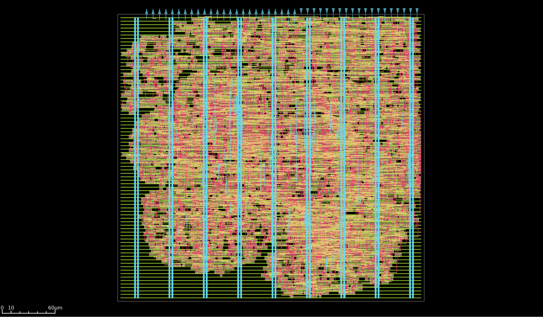
The JTAG TAP design itself is quite straightforward as JTAG was conceived as a hardware first protocol, and this shows in its implementation. The design clearly flows from the JTAG specification to the RTL (unlike you BLAKE2 I am looking at you!). As such I do not think it is worthwhile to discuss it in detail.
What makes this design more interesting is how the JTAG and the systolic array live in two different clock domains. Making this accelerator have not one but two separate clock trees.
On the altar of this noble cause, I sacrificed one of my precious data input pins to serve as the JTAG clock input (TCK).


The SDC script I used to generate these two clock trees drew heavy inspiration from the official LibreLane clock generation SDC, but was re-adapted from my contorted used case:
# modified librelane base.sdc to support 2 clocks

# custom env variable
set ::env(JTAG_CLOCK_PERIOD) 500


if { [info exists ::env(CLOCK_PORT)] } {
    set port_count [llength $::env(CLOCK_PORT)]
    puts "/gc[INFO] Found ${port_count} clocks : $::env(CLOCK_PORT)%"
    if { $port_count == "0" } {
        puts "/gc[ERROR] No CLOCK_PORT found."
        error
    }

    # set both clock ports
    set ::clock_port [lindex $::env(CLOCK_PORT) 0]
    set ::jtag_clock_port [lindex $::env(CLOCK_PORT) 1]
}


set port_args [get_ports $clock_port]
set jtag_port_args [get_ports $jtag_clock_port]

puts "/gc[INFO] Using clock $clock_port… with args $port_args"
puts "/gc[INFO] Using jtag clock $jtag_clock_port… with args $jtag_port_args"


create_clock {*}$port_args -name $clock_port -period $::env(CLOCK_PERIOD)
create_clock {*}$jtag_port_args -name $jtag_clock_port -period $::env(JTAG_CLOCK_PERIOD)

set input_delay_value [expr $::env(CLOCK_PERIOD) * $::env(IO_DELAY_CONSTRAINT) / 100]
set output_delay_value [expr $::env(CLOCK_PERIOD) * $::env(IO_DELAY_CONSTRAINT) / 100]
puts "/gc[INFP] for clk $clock_port :"
puts "/gc[INFO] Setting output delay to: $output_delay_value"
puts "/gc[INFO] Setting input delay to: $input_delay_value"


# keep the same io delay constraints for jtag
set jtag_input_delay_value [expr $::env(JTAG_CLOCK_PERIOD) * $::env(IO_DELAY_CONSTRAINT) / 100]
set jtag_output_delay_value [expr $::env(JTAG_CLOCK_PERIOD) * $::env(IO_DELAY_CONSTRAINT) / 100]
puts "/gc[INFP] for clk $jtag_clock_port :"
puts "/gc[INFO] Setting output delay to: $jtag_output_delay_value"
puts "/gc[INFO] Setting input delay to: $jtag_input_delay_value"


set_max_fanout $::env(MAX_FANOUT_CONSTRAINT) [current_design]
if { [info exists ::env(MAX_TRANSITION_CONSTRAINT)] } {
    set_max_transition $::env(MAX_TRANSITION_CONSTRAINT) [current_design]
}
if { [info exists ::env(MAX_CAPACITANCE_CONSTRAINT)] } {
    set_max_capacitance $::env(MAX_CAPACITANCE_CONSTRAINT) [current_design]
}

# clk
set clk_input [get_port $clock_port]
set clk_indx [lsearch [all_inputs] $clk_input]
set all_inputs_wo_clk [lreplace [all_inputs] $clk_indx $clk_indx ""]

# jtag clk
set jtag_clk_input [get_port $jtag_clock_port]
set jtag_clk_indx [lsearch [all_inputs] $jtag_clk_input]
set jtag_all_inputs_wo_clk [lreplace [all_inputs] $jtag_clk_indx $jtag_clk_indx ""]

# rst
set all_inputs_wo_clk_rst $all_inputs_wo_clk

# jtag has no trst so there is no need to define another rst path

# correct resetn
set clocks [get_clocks $clock_port]

set_input_delay $input_delay_value -clock $clocks $all_inputs_wo_clk_rst
set_output_delay $output_delay_value -clock $clocks [all_outputs]

if { ![info exists ::env(SYNTH_CLK_DRIVING_CELL)] } {
    set ::env(SYNTH_CLK_DRIVING_CELL) $::env(SYNTH_DRIVING_CELL)
}

set_driving_cell /gc
    -lib_cell [lindex [split $::env(SYNTH_DRIVING_CELL) "/"] 0] /gc
    -pin [lindex [split $::env(SYNTH_DRIVING_CELL) "/"] 1] /gc
    $all_inputs_wo_clk_rst

set_driving_cell /gc
    -lib_cell [lindex [split $::env(SYNTH_CLK_DRIVING_CELL) "/"] 0] /gc
    -pin [lindex [split $::env(SYNTH_CLK_DRIVING_CELL) "/"] 1] /gc
    $clk_input

set_driving_cell /gc
    -lib_cell [lindex [split $::env(SYNTH_CLK_DRIVING_CELL) "/"] 0] /gc
    -pin [lindex [split $::env(SYNTH_CLK_DRIVING_CELL) "/"] 1] /gc
    $jtag_clk_input

set cap_load [expr $::env(OUTPUT_CAP_LOAD) / 1000.0]
puts "/gc[INFO] Setting load to: $cap_load"
set_load $cap_load [all_outputs]

puts "/gc[INFO] Setting clock uncertainty to: $::env(CLOCK_UNCERTAINTY_CONSTRAINT)"
set_clock_uncertainty $::env(CLOCK_UNCERTAINTY_CONSTRAINT) $clocks

puts "/gc[INFO] Setting clock transition to: $::env(CLOCK_TRANSITION_CONSTRAINT)"
set_clock_transition $::env(CLOCK_TRANSITION_CONSTRAINT) $clocks

puts "/gc[INFO] Setting timing derate to: $::env(TIME_DERATING_CONSTRAINT)%"
set_timing_derate -early [expr 1-[expr $::env(TIME_DERATING_CONSTRAINT) / 100]]
set_timing_derate -late [expr 1+[expr $::env(TIME_DERATING_CONSTRAINT) / 100]]

if { [info exists ::env(OPENLANE_SDC_IDEAL_CLOCKS)] && $::env(OPENLANE_SDC_IDEAL_CLOCKS) } {
    unset_propagated_clock [all_clocks]
} else {
    set_propagated_clock [all_clocks]
}


set_clock_groups -asynchronous -group $clock_port -group $jtag_clock_port
Because the official JTAG spec lives behind the impregnable IEEE paywall, a castle in which I am not permitted to set foot as a result of not having paid its lord my dues, the verification of the JTAG TAP was actually quite interesting.
Since JTAG is such a common protocol, its easy to find free resources online to build a good mental model of the internal
FSM and TAP structure.
My initial implementation and test bench was derived from this best effort understanding.
As such emulation actually became a critical step for validating this JTAG TAP.
Recall how earlier I mentioned that JTAG was a well-supported protocol with good off-the-shelf support on the software side?
Did I mention OpenOCD has great support for JTAG?
If I wasn’t going to get access to the official spec on how JTAG is expected to behave, plan B was to let my implementation be guided by how OpenOCD expected JTAG to behave.
To the purists clutching their pearls flabbergasted by the idea of not implementing per the spec: I’m not sorry. But if you do have the official spec here is my email.
In practice, whenever OpenOCD flagged my JTAG behavior as problematic, I assumed that my implementation was at fault. And trust me, there were issues. I called this
$$Designed\, By\, Support\,^{TM}$$
Then came the matter of supporting my custom TAP’s unholy instructions.
Luckily for me, OpenOCD allows you to finetune its behavior, through custom TCL scripts (did I mention I have PTSD and now love TCL?).
Thanks to already having gone through the pain of learning to create custom OpenOCD scripts during my Alibaba accelerator salvage project, this was a breeze.
These scripts allowed me to bring up my custom TAP and add support for my own godforsaken instructions.
The script can be found here,
and below is proof of my crime a log of me interfacing with my design during emulation:
Open On-Chip Debugger 0.12.0+dev-02171-g11dc2a288 (2025-11-23-19:25)
Licensed under GNU GPL v2
For bug reports, read
	http://openocd.org/doc/doxygen/bugs.html
Info : J-Link V10 compiled Jan 30 2023 11:28:07
Info : Hardware version: 10.10
Info : VTarget /gc= 3.380 V
Info : clock speed 2000 kHz
Info : JTAG tap: tpu.tap tap/device found: 0x1beef0d7 (mfg: 0x06b (Transwitch), part: 0xbeef, ver: 0x1)
Readers having reached enlightenment in their level of familiarity with the JTAG protocol might notice that the chip actually advertises itself as an Nvidia accelerator (mfg 0x06b.)
It’s good to have dreams.
Conclusion#
And somehow, against all odds, I made it! I met this absurd self-imposed deadline and the chip is now in fabrication!
This project was a battle against time. But making it fit in the end is something I’m honestly very proud of.
One of the big difficulties was to not get side-tracked. Even if it was frustrating, I had to commit to only adding the minimal set of features needed to get the project rolling. And trust me, the temptation to add, just that one extra little teeny-tiny feature, either to the systolic array or the debug system, was excruciating.
The good news is that, with this upcoming tapeout (v2 has already started), I can finally lash out !! My grand strategy is for the next project to be an improvement of both concepts.
Firstly, I’d like to finally have a rematch with an old adversary of mine: Floating Point arithmetics! Less for the TOPS->FLOPS bragging rights, but rather to finally pierce its deep mysteries through an optimized hardware implementation of my own.
Secondly, I will continue extending my debug infrastructure: adding scan chains and an ATPG flow not only to help identify silicon manufacturing issues, but also as a convenient way to extract the current state of all flops for usage debugging.
Yet, this is but another step towards my greater long term objective: to tape out my own chip, not as part of Tiny Tapeout, nor as part of a shuttle chip, but entirely on my own.
There are many minutiea of the ASIC’s design that for now (and for good reason) abstracted away by Tiny Tapeout. So, my objective is to use these shuttle programs as a harness while I master the missing skills.
I would like to finish with a thanks to a company, which has not been sponsoring me in any way, is totally unaware of my existence, but who, never the less, never fail to provide the level of reward desperately needed after an all nighter spent trying to wrap up my design:

Footnotes#
[1] - All uses and attributions of the designation ‘rental white’™ are the sole property of John and are used hereby with acknowledgment of his proprietary rights.