
… we say tongue-in-cheek that TPU v1 “launched a thousand chips.”
In Google’s First Tensor Processing Unit - Origins, we saw why and how Google developed the first Tensor Processing Unit (or TPU v1) in just 15 months, starting in late 2013.
Today’s post will look in more detail at the architecture that emerged from that work and at its performance.
A quick reminder of the objectives of the TPU v1 project. As Google saw not only the opportunities provided by a new range of services using Deep Learning but also the huge scale and the cost of the hardware that would be needed to power these services, the aims of the project would be …
… to develop an Application Specific Integrated Circuit (ASIC) that would generate a 10x cost-performance advantage on inference when compared to GPUs.
and to …
Build it quickly
Achieve high performance
......at scale
...for new workloads out-of-the-box...
all while being cost-effective
Before we look at the TPU v1 that emerged from the project in more detail, a brief reminder of the Tensor operations that give the TPU its name.
Why is a Tensor Processing Unit so called? Because it is designed to speed up operations involving tensors. Precisely, what operations though? The operations are referred to … as a “map (multilinear relationship) between different objects such as vectors, scalars, and even other tensors”.
Let’s take a simple example. A two-dimensional array can describe a multilinear relationship between two one-dimensional arrays. The mathematically inclined will recognize the process of getting from one vector to the other as multiplying a vector by a matrix to get another vector.
This can be generalized to tensors representing the relationship between higher dimensional arrays. However, although tensors describe the relationship between arbitrary higher-dimensional arrays, in practice the TPU hardware that we will consider is designed to perform calculations associated with one and two-dimensional arrays. Or, more specifically, vector and matrix operations.
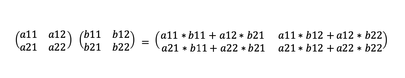
Let’s look at one of these operations, matrix multiplication. If we take two 2x2 matrices (2x2 arrays) then we multiply them together to get another 2x2 matrix by multiplying the elements as follows.
Why are matrix multiplications key to the operation of neural networks? We can look at a simple neural network with four layers as follows (only the connections from the first node in each later layer are shown for simplicity):
Where ‘f’ here is the activation function.
So the hidden and output layers are the results of applying the activation function to each element of the vector which is the result of multiplying the vector of input values times the matrix of weights. With a number of data inputs this is equivalent to applying the activation function to each entry in a matrix that is the result of a matrix multiplication.
As we’ve seen, the approach adopted by the TPU v1 team was an architecture first set out by H.T Kung and Charles E. Leiserson in their 1978 paper Systolic Arrays (for VLSI).
A systolic system is a network of processors which rhythmically compute and pass data through the system….In a systolic computer system, the function of a processor is analogous to that of the heart. Every processor regularly pumps data in and out, each time performing some short computation so that a regular flow of data is kept up in the network.
So how is the systolic approach used in the TPU v1 to efficiently perform matrix multiplications? Let’s return to our 2x2 matrix multiplication example.
If we have a 2x2 array of multiplication units that are connected in a simple grid, and we feed the elements of the matrices that we are multiplying, into the grid in the right order then the results of the matrix multiplication will naturally emerge from the array.
The calculation can be represented in the following diagram. The squares in each corner represent a multiply / accumulate unit (MAC) that can perform a multiplication and addition operation.
In this diagram, the values in yellow are the inputs that are fed into the matrix from the top and the left. The light blue values are the partial sums that are stored. The dark blue values are the final results
.Let’s take it step by step.
Step 1:
Values a11 and b11 are loaded into the top left multiply/accumulate unit (MAC). They are multiplied together and the result is stored.
Step 2:
Values a12 and b21 are loaded into the top left MAC. They are multiplied together and added to the previously calculated result. This gives the top left value of the results matrix.
Meanwhile, b11 is transferred to the top right MAC where it is multiplied by the newly loaded value a21 and the result is stored. Also, a11 is transferred to the bottom left MAC where it is multiplied by the newly loaded value b12, and the result is stored.
Step 3:
b21 is transferred to the top right MAC where it is multiplied by the newly loaded value a22 and the result is added to the previously stored result. Also, a12 is transferred to the bottom left MAC where it is multiplied by the newly loaded value b22, and the result is added to the previously stored result. In this step, we have calculated the top right and bottom left values of the results matrix.
Meanwhile, a12 and b21 are transferred to the bottom right MAC where they are multiplied and the result is stored.
Step 4:
Finally, a22 and b22 are transferred to the bottom right MAC where they are multiplied and the result is added to the previously stored value giving the bottom right value of the results matrix.
So the results of the matrix multiplication emerge down a moving ‘diagonal’ in the matrix of MACs.
In our example, it takes 4 steps to do a 2 x 2 matrix multiplication, but only because some of the MACs are not utilized at the start and end of the calculation. In practice, a new matrix multiplication would start top left as soon as the MAC is free. As a result the unit is capable of a new matrix multiplication every two cycles.
This is a simplified representation of how a systolic array works and we’ve glossed over some of the details of the implementation of the systolic array in TPU v1. I hope that the principles of how this architecture works are clear though.
This is the simplest possible matrix multiplication but can be extended to bigger matrices with larger arrays of multiplication units.
The key point is that if data is fed into the systolic array in the right order then the flow of values and results through the system will ensure that the required results emerge from the array over time.
Crucially there is no need to store and fetch intermediate results from a ‘main memory’ area. Intermediate results are automatically available when needed due to the structure of the matrix multiply unit and the order in which inputs are fed into the unit.
Of course, the matrix multiply unit does not sit in isolation and the simplest presentation of the complete system is as follows:
The first thing to note is that TPUv1 relies on communication with the host computer over a PCIe (high speed serial bus) interface. It also has direct access to its own DDR3 Dynamic RAM storage.
We can expand this to a more detailed presentation of the design:
Let’s pick some key elements from this presentation of the design, starting at the top and moving (broadly) clockwise:
DDR3 DRAM / Weight FIFO: Weights are stored in DDR3 RAM chips connected to the TPU v1 via DDR3-2133 interfaces. Weights are ‘pre-loaded’ onto these chips from the host computer’s memory via PCIe and can then be transferred into the ‘Weight FIFO’ memory ready for use by the matrix multiply unit.
Matrix Multiply Unit: This is a ‘systolic’ array with 256 x 256 matrix multiply/accumulate units that is fed by 256 ‘weight’ values from the top and 256 data inputs from the left.
Accumulators: The results emerge from the systolic matrix unit at the bottom and are stored in ‘accumulator’ memory storage.
Activation: The activation functions described in the neural network above are applied here.
Unified Buffer / Systolic Data Setup: The results of applying the activation functions are stored in a ‘unified buffer’ memory where they are ready to be fed back as inputs to the Matrix Multiply Unit to calculate the values needed for the next layer.
So far we haven’t specified the nature of the multiplications performed by the matrix multiply unit. TPU v1 performs 8-bit x 8-bit integer multiplications, making use of quantization to avoid the need for more die-area-hungry floating-point calculations.
The TPU v1 uses a CISC (Complex Instruction Set Computer) design with around only about 20 instructions. It’s important to note that these instructions are sent to it by the host computer over the PCIe interface, rather than being fetched from memory.
The five key instructions are as follows:
Read_Host_Memory
Reads input values from the host computer’s memory into the Unified Buffer over PCIe.
Read_Weights
Read weights from the weight memory into the Weight FIFO. Note that the weight memory will already have been loaded with weights read from the computer’s main memory over PCIe.
Matrix_Multiply / Convolve
From the paper this instruction
… causes the Matrix Unit to perform a matrix multiply or a convolution from the Unified Buffer into the Accumulators. A matrix operation takes a variable-sized B*256 input, multiplies it by a 256x256 constant weight input, and produces a B*256 output, taking B pipelined cycles to complete.
This is the instruction that implements the systolic array matrix multiply. It can also perform convolution calculations needed for Convolutional Neural Networks.
Activate
From the paper this instruction
Performs the nonlinear function of the artificial neuron, with options for ReLU, Sigmoid, and so on. Its inputs are the Accumulators, and its output is the Unified Buffer.
If we go back to our simple neural network model the values in the hidden layers are the result of applying an ‘activation function’ to the sum of the weights multiplied by the inputs. ReLU and Sigmoid are two of the most popular activation functions. Having these implemented in hardware will have provided a useful speed-up in the application of the activation functions.
Write_Host_Memory
Writes results to the host computer’s memory from the Unified Buffer over PCIe.
It’s probably worth pausing for a moment to reflect on the elegance of these five instructions in providing an almost complete implementation of inference in the TPU v1. In pseudo-code, we could describe the operation of the TPU v1 broadly as follows:
Read_Host_Memory
Read_Weights
Loop_Start
    Matrix_Multiply
    Activate
Loop_End
Write_Host_Memory
It’s also useful to emphasize the importance of the systolic unit in making this possible and efficient. As described by the TPU v1 team (and as we’ve already seen):
.. the matrix unit uses systolic execution to save energy by reducing reads and writes of the Unified Buffer …. It relies on data from different directions arriving at cells in an array at regular intervals where they are combined. … data flows in from the left, and the weights are loaded from the top. A given 256-element multiply-accumulate operation moves through the matrix as a diagonal wavefront.
The TPU v1’s hardware would be of little use without a software stack to support it. Google developed and used Tensorflow so creating ‘drivers’ so that Tensorflow could work with the TPU v1 was the main step needed.
The TPU software stack had to be compatible with those developed for CPUs and GPUs so that applications could be ported quickly to the TPU. The portion of the application run on the TPU is typically written in TensorFlow and is compiled into an API that can run on GPUs or TPUs.
Like GPUs, the TPU stack is split into a User Space Driver and a Kernel Driver. The Kernel Driver is lightweight and handles only memory management and interrupts. It is designed for long-term stability. The User Space driver changes frequently. It sets up and controls TPU execution, reformats data into TPU order, translates API calls into TPU instructions, and turns them into an application binary.
As we saw in our earlier post, the TPU v1 was fabricated by TSMC using a relatively ‘mature’ 28nm TSMC process. Google has said that the die area is less than half the die area of the Intel Haswell CPU and Nvidia’s K80 GPU chips, each of which was built with more advanced processes, that Google was using in its data centers at this time.
We have already seen how simple the TPU v1’s instruction set was, with just 20 CISC instructions. The simplicity of the ISA leads to a very low ‘overhead’ in the TPU v1’s die for decoding and related activities with just 2% of the die area dedicated to what are labeled as ‘control’.
By contrast, 24% of the die area is dedicated to the Matrix Multiply Unit and 29% to the ‘Unified Buffer’ memory that stores inputs and intermediate results.
At this point, it’s useful to remind ourselves that the TPU v1 was designed to make inference - that is the use of already trained models in real-world services provided at Google’s scale - more efficient. It was not designed to improve the speed or efficiency of training. Although they have some features in common inference and training provide quite different challenges when developing specialized hardware.
So how did the TPU v1 do?
In 2013 the key comparisons for the TPU v1 were with Intel’s Haswell CPU and Nvidia’s K80 GPU.
And crucially the TPU v1 was much more energy efficient that GPUs:
In the first post on the TPU v1, we focused on the fact that an organization like Google could marshal the resources to build the TPU v1 quickly.
In this post we’ve seen how the custom architecture of the TPU v1 was crucial in enabling it to generate much better performance with much lower energy use than contemporary CPUs and GPUs.
The TPU v1 was only the start of the story. TPU v1 was designed quickly and with the sole objective of making inference faster and more power efficient. It had a number of clear limitations and was not designed for training. Both inside and outside Google firms would soon start to look at how TPU v1 could be improved. We’ll look at some of its successors in later posts.
After the paywall, a small selection of further reading and viewing on Google’s TPU v1.