The beginning
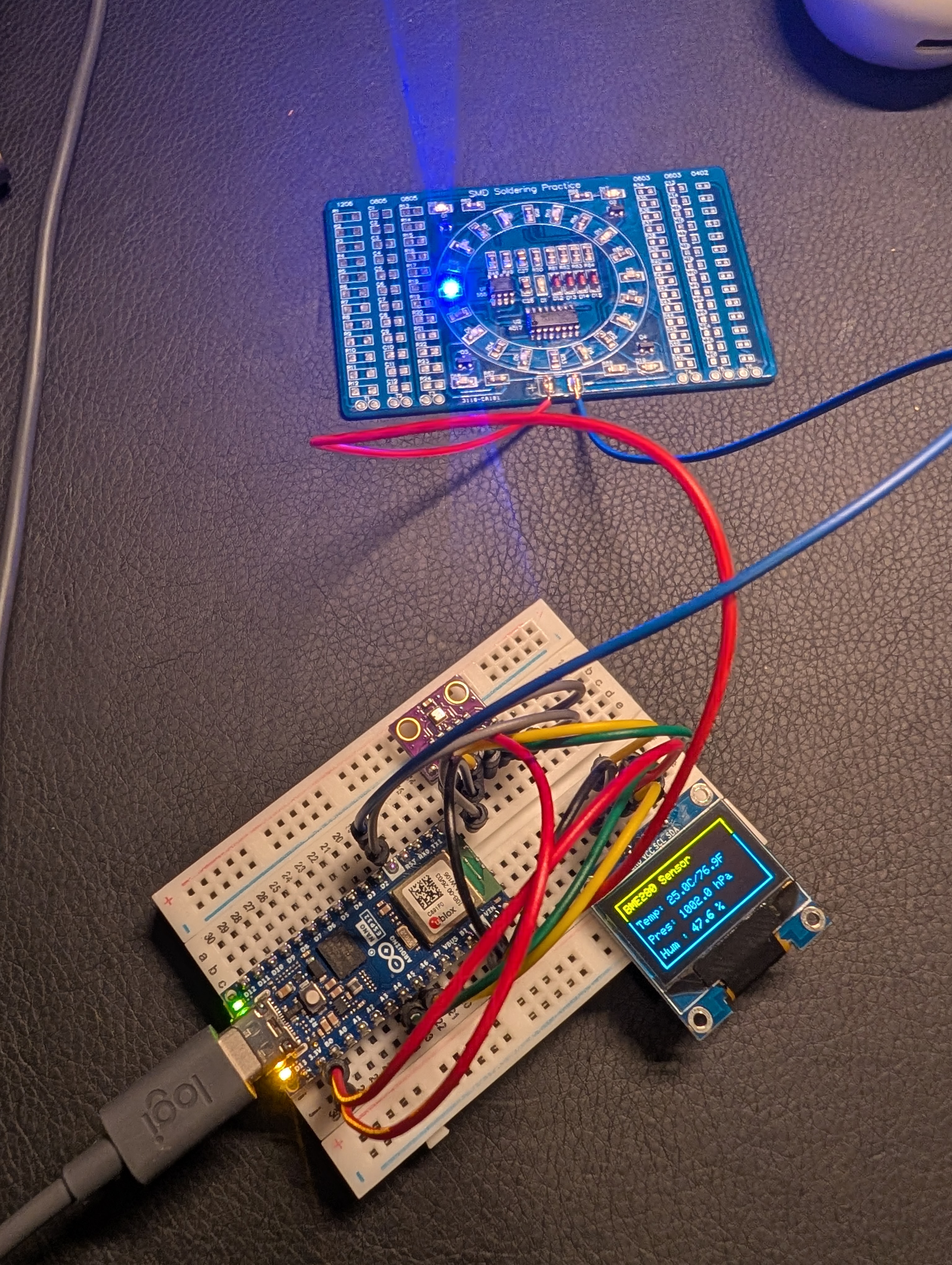
About a couple months ago I purchased an Arduino Nano ESP32 dev board. I had this sudden itch and I wanted to play around with hardware. I don't really have much experience in this space, besides working on firmware for an IoT company over a decade ago, but I've written tons of software over the years. I was very surprised how quickly I was able to get the built-in LEDs to blink with Arduino IDE and some help from LLMs. After that I moved on to figure out how to build and flash firmware directly from the command line without having to deal with all these custom abstractions. I like operating from CLI. That was also somewhat easy and gave me confidence that I can go back to my normal tools (nvim) for working with code.
The devboard itself does not have much going on. Next was getting some peripherals so I ordered a small LCD and BME280 temperature/humidity sensor breakout boards. Both of these I was able to wire up to the ESP32 chip and get them to talk over the I2C protocol.

Naturally, we cannot continue assembling pre-existing modules for a variety of reasons. I think they are great for prototyping, but I like getting out of the prototyping phase as soon as possible and getting into a more "release" or "production" workflow. I was thinking maybe I should recreate the Arduino board with all these components hardwired so I can ditch the breadboard. That sounded great, but it felt a little bit ambitious. There's lots of components and it would make it hard for me to test everything. Instead, I decided to create the BME280 sensor module. This would let me get a feel for what it takes to design something starting with schematics and ending up with a custom PCB. In the picture above you can see the small brown board that I got from Amazon, that's a BME280 sensor board which only has a handful of components. If everything goes as planned I should be able to swap-in my custom board and everything should continue working as before. That was the plan.
Schematic and PCB design
There seem to be several tools available for schematic/pcb design. I needed something that's free and runs on Mac OS. Some people praise EasyEDA, others like KiCad. I didn't do much research on this topic, it seemed like either of them would fit the bill, but I picked KiCad since it's free GPL licensed software.
All sensors, chips and components come with what's called a datasheet. A datasheet is a technical document made available by the manufacturer describing how the component functions, at what temperatures it can operate, reflow (soldering) temperature curves, size and exact dimensions, example wiring and many other things depending on the component.
For my sensor module, I needed to wire the BME280 for an I2C interface to make it plug-and-play. The module that I purchased from Amazon actually supports both I2C and SPI. So what I'm doing is not an exact copy, but actually a more narrow implementation. The BME280 datasheet has pin-out and connection diagrams starting on page 38. It actually provides examples for both SPI and I2C connections. I took the provided I2C connection diagram and transferred it to KiCad.

I wouldn't call KiCad the most intuitive application for first-time users. However, I was able to draw up the exact schematic as was shown on the datasheet.
To transfer a schematic to a PCB you need to select what's called a footprint for each component. For example, there's only one type of BME280 sensor and it really has only one shape/size (aka footprint) available. That's not the case for other types of general use components such as resistors or capacitors. What footprints you pick will dictate the size of your board, how easy it is to assemble and most likely many other factors that I'm not aware of (such as heat dispersion).
Through my research I discovered that most commonly you're going to encounter SMD and THT components. THT or through-hole components are more old-school looking tech (though it's not old), generally larger in size and they get installed by pushing component legs through the holes in the PCB and soldering the legs to the board after. This can be done in most cases with a regular soldering iron.
SMD stands for surface mounted devices and are what you'd find in almost all modern electronic devices. They are much smaller in size, and as the size gets smaller, they will require more specialized equipment for installation. When I started looking at the footprint library in KiCad I got very confused because it wasn't immediately clear to me whether I needed to find a footprint for the exact component brand that I was planning to use or not. Lots of general SMD components have standardized footprints, I discovered. They follow standard codes like 1206, 0805, 0603, etc which translate to dimensions 0.12" by 0.06" or (3.2mm x 1.55mm) for a 1206 component. I went with the 0805 size as this seemed to be suitable for hand soldering, though it's pushing the limits.
After you assign a footprint for each component you can then import them into the PCB editor and layout your PCB.


The layout process did not seem too complicated, however, you need to be aware of how you are routing the connections, or they could otherwise prevent other ones from getting to their destination. I was able to layout everything on the front layer of the board. The only thing I did special (maybe that is not so special) was ground filling empty space on the front and back and then connecting front to back using via. This seems to be a common pattern used in the PCB design. Otherwise, it can get really tricky to route the connections without blocking other ones, even for a small simple board like the one I'm making here.
Sourcing components and ordering PCB
The component search was somewhat interesting too. I purchased my components from DigiKey. Although, it's probably best to have accounts with several electronics shops, just in case there's a limited inventory. I was able to find all components on DigiKey except for the BME280 sensor itself. The BME280 sensor was out of stock on several sites and it looked like it would take several months to get the backorder processed. I skipped the BME280 and decided to rip it off from the Amazon module I purchased earlier. The resistors and capacitors were somewhat easy to find, I just had to be careful picking the correct footprint and configuration (resistance etc).
KiCad also lets you generate a bill of materials (BOM). It's just a list of components and their configuration and where they need to be placed. The PCB manufacturers can sometimes perform the assembly for you if you provide them with the BOM. I did not do that, I wanted to hand assemble to get a feel for it.

To order a PCB you need to export gerber and drill files. The gerber files define trace layout and the drill file is for the CNC machining. I exported both of these with default settings and packaged them into a zip file which I then provided to JLCPCB. From there you finish the order form. I did not make many changes and used defaults. JLCPCB is a Chinese company, order to door took about 2-3 weeks and cost me under $10 dollars. There are faster options, but they would break the bank on delivery costs.
My tools and assembly
As part of my current homelab, I only have two soldering tools plus a multimeter.
Hakko FX888DX-010BY

I purchased this iron because it lets you control the temperature and it has pretty good reviews. It heats up really fast. I usually run my iron at 650F. However, temperature adjustment is critical so you know exactly what temperature you're getting so you don't damage the components.
Quick 861DW

This device is called a hot air station, sometimes reflow or rework station. It is used heavily in electronics repair shops to replace components. You also can use it to solder SMD components. Once you go below 1206, using a soldering iron gets tricky. The way SMDs get soldered is by spreading solder paste over connections, placing the components on top and then microwaving the board using a hot plate or hot air gun to melt the solder. The hot air gun is the most versatile tool and it's good for smaller assembly.
I picked up a Quick 861DW because it's considered a pro entry-level device (according to LLMs at least). The most important part for a device like this is airflow control. I run this device on airflow setting 15 (which is very low volume) and 250C. SMDs are tiny and very light devices, anything that does not give you good air control will blow away the components.
The assembly
It took me about 15 minutes to assemble the board. That involved desoldering the BME280 sensor from the Amazon board, applying solder paste and laying out the components and soldering everything up. The only thing I struggled with was the sensor. The sensor is tiny and it has 8 connection pads underneath it so I wasn't sure if I would short any of the connections by accident because I couldn't see what was going on under the chip. I kept the area for the sensor clean and made sure there was flux on it and I left the rest to the surface tension gods.

The results
I was giving this whole thing a 50/50 chance of working on the first try. I wasn't even sure if I routed everything correctly on the PCB. The "via" and grounding were a bit confusing. Then, soldering the sensor was slightly tricky and I wasn't sure if I shorted connections anywhere. However, to my surprise, the board I designed and assembled was plug-and-play on the first try!

I did not have to modify the firmware, I did not have to put anything in between the board. It was literally a plug-and-play experience because I exposed the same I2C interface that I used originally.
This experience gave me confidence that I can produce custom and working PCBs. This, of course, was a very simple project, but it took me through the whole process end-to-end. It gave me a better understanding of the steps I may need to take for more complex designs. I was thinking maybe for the next one I should place the LCD, ESP32 and BME280 on a single board, hardwired. This one sounds a bit more complex. How do you flash the chip? How do you supply power? What is necessary and what is not? For example, the Arduino Nano dev board has lots of components on it. Are all of them needed? I have no idea. I will see what I'll do next, but I enjoyed this experience.