The MMI 5300 was a memory chip from the early 1970s, storing 1024 bits in tiny fuses.1 Unlike regular RAM chips, this was a PROM (Programmable Read-Only Memory); you programmed it once by blowing fuses and then it held that data permanently. The chip I examined originally cost $70 and was built by MMI (Monolithic Memories Incorporated), a leading PROM manufacturer at the time.
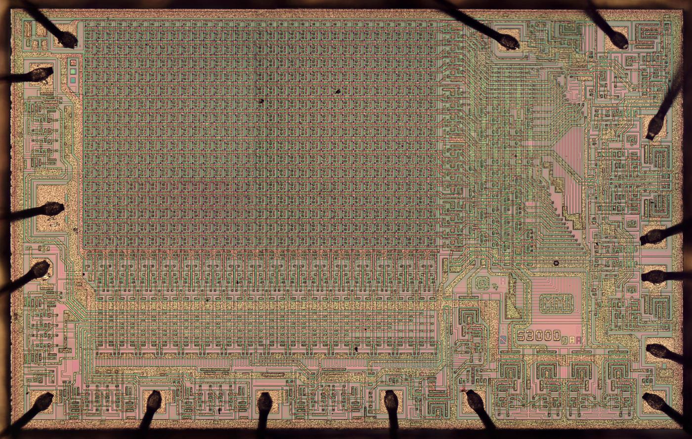
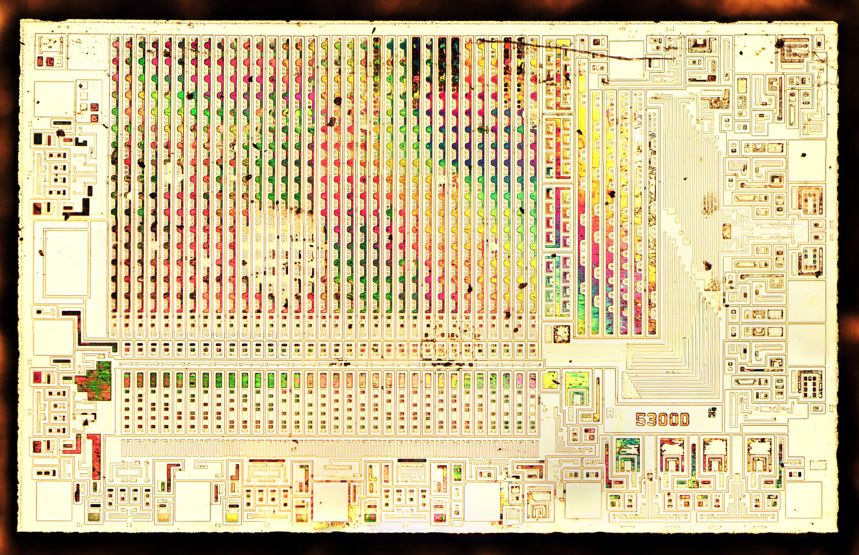
The highly magnified photo below shows the chip's silicon die. The metal layer on top of the silicon is most visible in this photo; the transistors and resistors fabricated from silicon are underneath. The wires around the edges are the 16 bond wires between the silicon die and the external pins. In the upper left, the 1024 bits of data are stored in a 33×33 array of diodes and fuses. (I'll explain the extra row and column below.) This chip is built from NPN transistors, unlike the MOS transistors used in most modern chips.
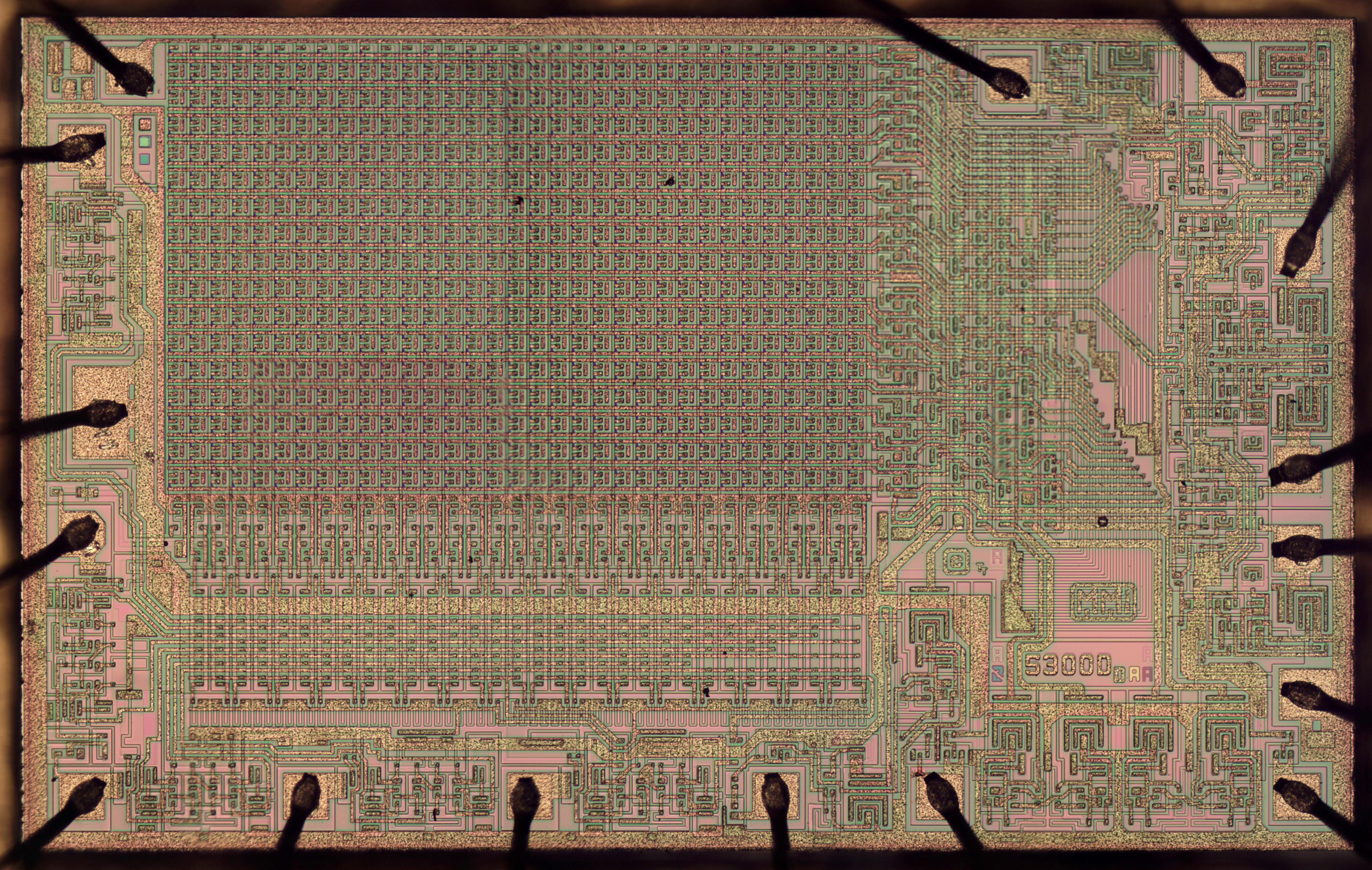
Die of the MMI 5300 PROM chip, holding 1024 bits of information. Click image for a larger version.
To produce the die photo, I started with the chips below, in their 16-pin ceramic packages; the 5300 and 6300 chips are essentially the same.2 Since the chips were in ceramic packages, I could decap the chip simply by knocking the metal lid off with a chisel, revealing the silicon die.

The MMI 5300 and 6300 PROM chips are in ceramic packages. The chips have 1974 and 1973 date codes.
In the photo below, the silicon die is mounted very off-center in the package. It's unclear if that is intentional or sloppy manufacturing. Tiny bond wires connect the die to the metal contacts of the package.

The MMI 5300 PROM with the lid removed, exposing the die.
Inside the chip
The diagram below shows the main parts of the chip, with the pins labeled. The chip stores 1024 bits as 256 4-bit words. The 8 address lines A0-A7 select one of the 256 words, and the bits are output on pins Out1-Out4. The Program pin is used to store data in the chip by blowing fuses. The Vcc and ground pins power the chip.
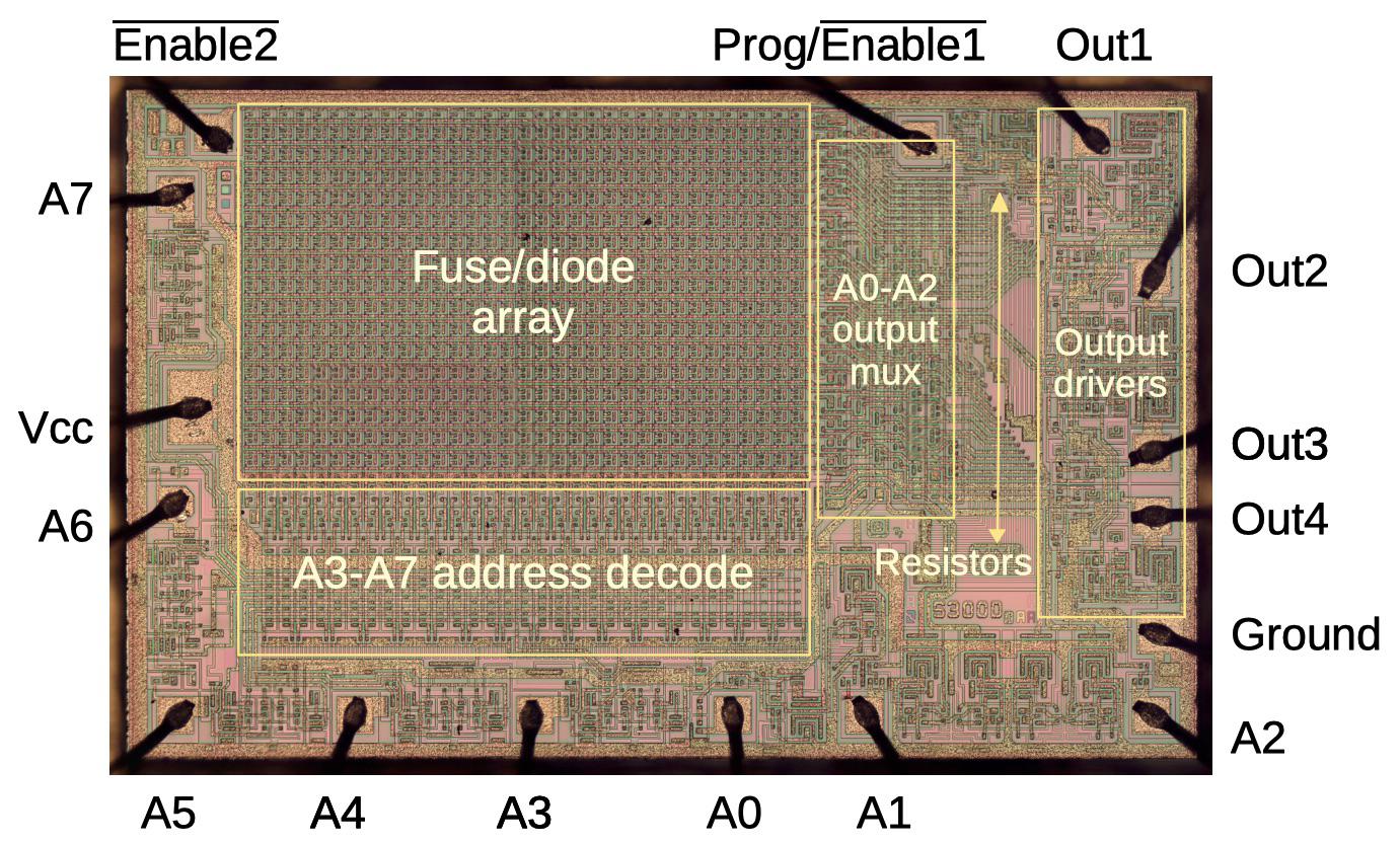
Die of the 5300 PROM with components labeled.
The 1024 bits of data are stored in a 33×33 array of diodes and fuses. Note that the data array only takes up about a quarter of the chip; the rest of the chip holds the supporting circuitry. Below the data array, address decode circuitry used the address lines to select one of 32 columns in the array. To the right, DTL multiplexers4 reduced the 32 rows of output to the 4 desired outputs. The output drivers amplified these signals and sent them to the output pins.
The fuses
The chip stored data in tiny fuses. An intact fuse represented a 1, while a blown fuse represented a 0. Thus, the chip was shipped containing all 1's, and the user programmed the chip by blowing fuses where a 0 bit was required. The fuses were fabricated from tiny regions of Nichrome metal that heat up and melt under high voltage. (Nichrome is a nickel-chromium alloy that has much higher resistance than typical metals, causing it to heat up. It is commonly used in applications such as toasters.)
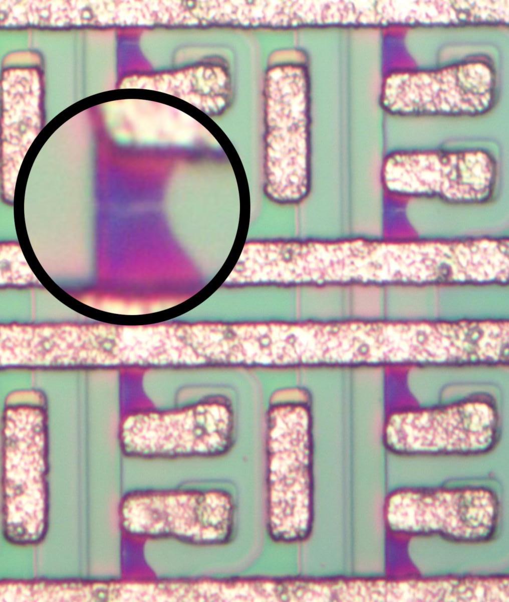
A closeup of the fuses (purple) that store data. Inset circle shows a magnified fuse, showing the tiny horizontal crack indicating the fuse was blown.
The fuses are visible in the die photo above; they are the purple regions between the metal wiring. The fuses are very small, about 8µm long. I expected a blown fuse would vaporize entirely, but instead a blown fuse contains a tiny crack roughly 700 nm wide. (This is the wavelength of red light, so the crack is just barely visible under the microscope.)
Address decoding
The PROM stored 1024 bits as 256 words of 4 bits. However, the bits are physically arranged in a 33×33 grid since a square memory grid is more efficient than a highly-rectangular one. To access the memory, address bits A3-A7 select one of the 32 columns. The selected 32 bits in the column go through the multiplexers at the right, which select one bit out of each group of eight, based on address bits A0-A2. The four selected bits become the four outputs. Thus, addressing has two parts—one to select the column and one to select the four output bits—and they have separate circuitry,
Column selection uses 32 NAND gates, implemented with multiple-emitter transistors.3 (The N and P silicon regions of the transistors are visible as rectangular boxes, with the brownish metal layer on top connecting the regions together.) Each NAND gate has a different combination of address bits A3-A7 either inverted or uninverted, so each address activates a different NAND gate, selecting the associated column. You can see the binary counting in the emitters. The A7' and A7 lines alternate connections every column. The A6'/A6 connections alternate every two columns, while A5'/A5 alternate every four, and so on.

Part of the column address decoder. Each (vertical) transistor decoded a particular address, determined by which address lines are connected to the emitters. There were 32 columns in total.
The data array consists of a diode and fuse for each bit. (Without diodes, the bits would all be shorted together.) If the fuse is present, a low signal on the selected column will pull the corresponding row low through the diode (indicating a 1). If the fuse is blown, the row will remain high (indicating a 0). Thus, by blowing fuses, bits are programmed into the memory array. The diodes themselves are mostly hidden under the metal layer below. The column select lines run vertically in the silicon under the metal layer; the metal stripes on top reduce the resistance.
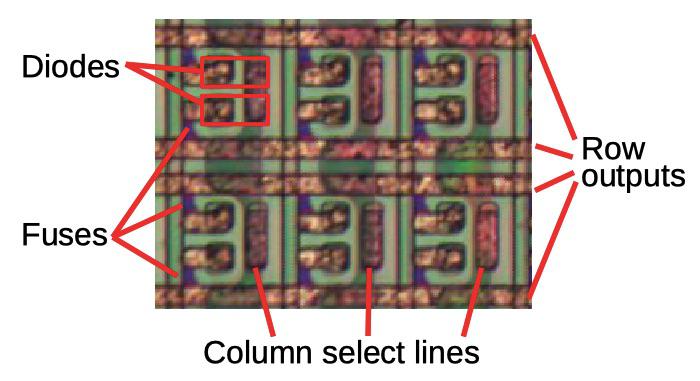
12 bits in the memory array. Each bit has a diode and fuse between a column select line and a row line.
Programming
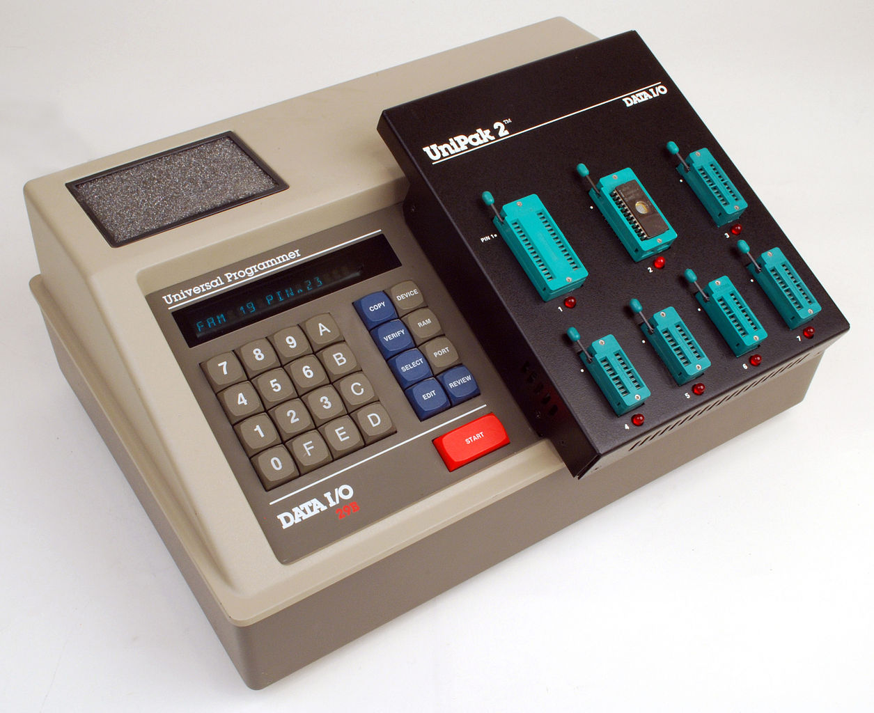
To program the PROM, the user melted the necessary fuses one at a time using carefully-controlled high voltage pulses. After selecting the desired address, 27 volts was applied to the programming pin (a much higher voltage than the typical 5V TTL level). After a carefully-timed interval, the desired output was brought to 20 volts for a few microseconds to blow the fuse. (The timing and voltages needed to be precise so the fuse would blow without damaging other parts of the chip.) The process was repeated for each desired 0 bit. Customers used a PROM programmer such as shown below to perform these operations automatically.

For the most part, reading a fuse and blowing a fuse used the same circuitry; the difference was the output pin circuit, which could either output a bit or sink a large current to blow the fuse, depending on the programming mode.5 The transistors along the programming path were larger than regular transistors to handle the larger current. For example, the diagram below compares the multiplexer NPN transistors to a typical NPN transistor on the chip. Also note that the 8 transistors in a multiplexer share a single collector (the multiplexer output).

Eight transistors in a multiplexer (left) compared to a typical NPN transistor (right). The metal layer was removed for this photo. The remaining oxide gives the transistors a colored appearance. N-doped silicon appears darker.
Testing
Before examining this chip, I didn't consider how difficult it was for the manufacturer to test a PROM. Most chips can be extensively tested before shipping to the customer, but you can't test the PROM fuses without irreversibly programming the chip. Even testing the address decode logic is difficult; since the chip is manufactured with all 1's, you'd read the same result even if the address circuitry is broken.
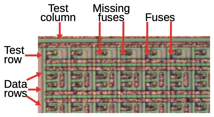
The chip included an extra row and column of fuses for testing.
To support testing, the chip contains an extra row and column of fuses.6 As a result, the storage grid was 33×33, rather than the 32×32 grid you'd expect. Half of the test fuses were missing, so reading the correct pattern of 0's and 1's tested the address decoders. By blowing test fuses and reading the results, the programming characteristics could be tested. The datasheet says that the chips should have a programming yield of over 95%. Compared to most integrated circuits, this is a high failure rate, but it's understandable given the difficulties of testing the chip.
Unused circuitry
One interesting feature of the 5300 die is that it has some transistors that aren't connected to anything else in the chip. The diagram below shows some of the unused transistors in the output circuitry. There are no metal connections from these transistors to the rest of the chip, making them apparently useless.
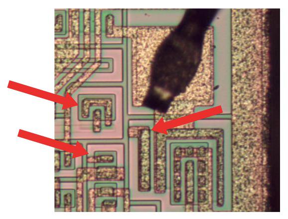
The output driver circuitry has some unused transistors, marked with arrows.
The reason for these unused transistors is that the same silicon layout could be used for slightly different PROM chips, depending on how the metal layer was wired up. The 5300 PROM had open-collector outputs, but a tri-state version (6301) was also available.7 Both chips used the same silicon die, but had small modifications to the metal layer to wire the transistors differently. Since the 5300 didn't need output transistors to pull the output to 1, these were left unconnected, yielding the unused circuitry seen above.
Conclusion
PROM chips were an important part of early computer systems, often holding the boot code, but their popularity peaked in the early 1980s as they were replaced by erasable PROM (EPROM) chips. EPROM chips had a distinctive quartz window over the die; shining ultraviolet light on the chip erased it, so it could be reused. EPROMs in turn were replaced by electrically-erasable PROMs (EEPROMs), similar to flash memory. To see how much technology has improved, consider that the 6300 PROM chip cost $70 in 1971 and stored 128 bytes. Now you can get a 128 GB flash drive for under $20: a billion times the storage, plus you can write it more than once.
Die with the metal stripped off to expose the silicon. This makes the structure of the transistors visible. The thin remaining oxide layer produces a rainbow effect in some areas.
I announce my latest blog posts on Twitter, so follow me @kenshirriff for future articles. I also have an RSS feed. Thanks to Marc Verdiell for supplying the chip.