To use the Montreal subway (the Métro), you tap a paper ticket against the turnstile and it opens. The ticket works through a system called NFC, but what's happening internally? How does the ticket work without a battery? How does it communicate with the turnstile? And how can it be so cheap that you can throw the ticket away after one use? To answer these questions, I opened up a ticket and examined the tiny chip inside.
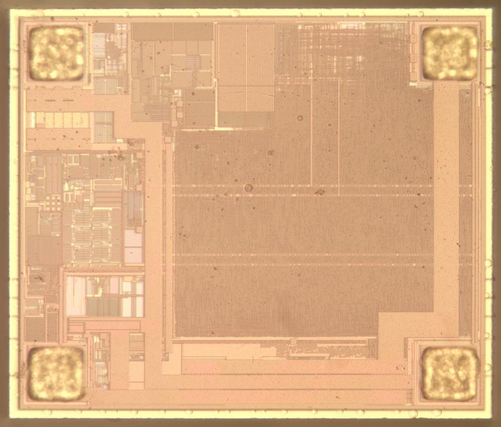
The image below shows the chip inside the ticket, highly magnified. The four golden squares in the corner are the connections to the antenna. The tan-colored lines are the metal wiring layer on top of the chip; the thickest lines wire the antenna to other parts of the chip. The darker region that takes up the majority of the chip is the chip's digital logic. To the left is the analog circuitry that handles the signal from the antenna.
 for a larger view.")
The MIFARE Ultralight die under the microscope. (Click this image (or any other) for a larger view.
The chip uses NFC (Near-Field Communication). The idea behind NFC is that a reader (i.e. the turnstile) and an NFC tag (i.e. the ticket) communicate over a short distance through magnetic fields, allowing them to exchange data. The reader generates a magnetic field that both powers the tag and sends data to the tag. Both the reader and the tag have coil-like antennas so the reader's magnetic field can be picked up by the tag.1 When you tap your ticket on the turnstile, the NFC communication happens in 35 milliseconds, faster than an eyeblink. The data provided by the NFC tag shows that you have a valid ticket and then you can enter the subway.
The photo below shows the subway ticket, made of printed paper.2 At the right, the ticket appears to have golden smart-card contacts, like a credit card with an EMV chip. However, those contacts are completely fake, just printed onto the card with ink, and there is no chip there. Presumably, the makers thought that making the card look like a smart card would help people understand it. The card actually uses an entirely different technology.

A Montreal subway card. This card is for occasional use and is disposable. Regular travel uses a rigid plastic card containing a different chip.
Although the subway card is paper on the outside, its core is a thin plastic sheet, shown below. The sheet has a coiled antenna made from a layer of metal foil. If you look closely, you can see the tiny NFC chip in the lower right, a black speck connected to two sides of the antenna wire.3 The diagonal metal stripe in the upper left makes the antenna into a loop; topologically, a spiral antenna won't work on a 2-D sheet, so the diagonal bridge completes the circuit.

The antenna and chip inside the subway card.
I want to emphasize the absurdly small size of the chip: 570 µm × 485 µm. The photo below shows that it is about the size of a grain of salt. The chip is also extremely thin—75 µm or 120 µm—so you can't even feel the chip inside the ticket.

The chip next to grains of salt. I composited two images, one illuminated from above to show the die and one illuminated from below to show the salt.
Functions of the chip
There are many different types of NFC chips with varying levels of functionality. 4 This one is called the MIFARE Ultralight EV1,5 a low-cost chip designed for one-time ticketing applications. The basic function of the Ultralight chip is simple: providing a block of data to the reader. The chip holds its data in a small EEPROM; this chip has 48 bytes of user memory, while another variant has 108 bytes of user memory.
The Ultralight chip lacks the cryptography support found in more advanced chips. The Ultralight isn't much more secure than a printed ticket with a QR code or barcode, like you'd download for a show. It's up to the reader to validate the data and make sure the same ticket isn't being used multiple times.6
The Ultralight chip has a few features beyond a printed ticket, though. The chips are manufactured with a unique 7-byte identification code (UID). Moreover, the UID is signed, ensuring that fake UIDs cannot be generated.7 The chip also supports password-protected memory access and locking of memory pages to prevent modification. Since the password is transmitted without encryption, the security is weak, but better than nothing.8
Another interesting feature of the chip is the one-way counter. The chip has three 24-bit counters that can be incremented but not decremented. The counters can be used to allow the ticket to be used a particular number of times, for instance.9
Photographing the chip
To photograph the chip, I went through several steps to remove the chip from the ticket and then strip the chip down to the bare silicon. First, to extract the plastic sheet with the chip and the antenna from the paper ticket, I simply soaked the ticket in water. This turned the paper into mush, which could be scraped off to reveal the plastic core. Next, I cut out a small square of plastic that included the chip and put it in boiling sulfuric acid for about 30 seconds. This removed the plastic and adhesive, leaving the silicon die. (I try to avoid boiling acids, but processing a tiny chip like this only required a few drops of sulfuric acid, minimizing the risk.)
The die was covered with a passivation layer to protect its surface, a sandwich of silicon nitride and PSG (phosphosilicate glass) 1.1 µm thick according to the datasheet. The chip's underlying circuitry was visible, but slightly hazy due to this layer. I removed the passivation layer by boiling the chip in phosphoric acid for a few minutes. The image below shows the chip after this step. The top metal layer is much more visible, although some of the metal was dissolved by the acid. The thick metal lines connect the four bond pads to various parts of the analog circuitry, while many thin vertical metal lines provide interconnections of the logic circuitry.

The die after treatment with phosphoric acid to remove the passivation layer. Click for a much larger version.
Next, I treated the die with several cycles of treatment with Armour Etch to dissolve the oxide layer and hydrochloric acid to dissolve the metal. I think the chip had three layers of metal wiring on top of the silicon. Unfortunately, my process doesn't remove the metal layers cleanly, but causes them to come off in chaotic tangles. Since I wasn't interested in tracing the circuitry layer-by-layer, this wasn't a significant problem.
With the metal layers and polysilicon removed, I was left with the bare silicon. At this point, the underlying structure of the chip is visible. The doped silicon regions show the transistors, although they are extremely small at this scale. The white rectangles are capacitors. The chip has capacitors for many reasons: producing the right resonant frequency with the antenna, filtering the power, and boosting the voltage with charge pumps.

The die after stripping it down to the silicon.
My biggest concern while processing this chip was to avoid losing it. With a chip this small, bumping the chip or even breathing on it can send the chip flying perhaps never to be seen again. Even trying to pick up the chip with tweezers is risky, since it can easily pop out and disappear. It's no fun examining the floor, inch by inch, trying to figure out if a speck is the lost chip or a bit of dirt. I found that the best way to move the chip between processing and a microscope slide was to put the chip in a few drops of water and move it with a pipette. Even so, there were a couple of times that I lost track of the chip and had to check some specks under the microscope to determine which was the chip and which were dirt.
Overview of the chip
The block diagram below shows the high-level structure of the chip. At the left, the antenna is connected to the RF interface, the analog circuitry that converts the high-frequency signals into digital data. This circuitry also extracts power from the antenna's signal to power the chip.

The majority of the chip contains digital logic to process the 18 different commands that it can receive from the reader.
Some commands, such as Wake-up or Halt control the chip's state.
Other commands, such as Read or Write provide access to the EEPROM storage.
The specialized Read_Cnt and Incr_Cnt commands access the chip's counters.
The chip has an "intelligent anticollision function" that allows multiple cards to be read without conflict if they are presented to the reader simultaneously. If a conflict is detected, the reader uses a standard NFC algorithm to select the cards one at a time, based on their identification numbers. The anticollision algorithm uses four of the chip's commands.
Finally, the chip has an EEPROM to store its data. Unlike RAM, the EEPROM holds data even when unpowered; it is designed to hold data for 10 years. To store data in the EEPROM, it must be written with a higher voltage than the rest of the chip uses. The EEPROM interface circuit produces the necessary signals.
The diagram shows the chip with its functional blocks labeled. The majority of the die is occupied with digital logic; I'll explain below how it is implemented with standard-cell logic. At the top is the EEPROM, a square of storage cells. To the right of the EEPROM is a charge pump, a circuit to boost the voltage through switched capacitors. The EEPROM interface circuitry is between the EEPROM and the digital logic.

The die, stripped down to the silicon, with presumed functional blocks labeled.
The remainder of the chip contains analog circuitry that is harder to interpret, so my labels are somewhat speculative. The four bond pads are where the antenna is connected to the chip. There are four pads to support two parallel antennas if desired. The first die photo shows the metal wiring between the bond pads and the structures that I've labeled as RF transistors and RF diodes. The "RF transistors" in the upper left are large, oval-shaped structures. These may be the transistors that send data back to the reader by modifying the load. Alternatively, they could be Zener diodes to regulate the voltage powering the chip, since Zener diodes often have an oval shape. The "RF diodes" at the bottom may rectify the signal from the antenna, producing the power for the chip. The rectified signal is also demodulated and processed by the analog logic to extract the digital data sent from the reader.
Sending data from the tag to the reader: load modulation
You might expect the tag to send data back to the receiver by transmitting a signal through the antenna. However, transmitting a signal takes power and the tag doesn't have much power available, just the power that it extracts from the reader's signal. Instead, the tag uses a clever technique called load modulation to send data to the reader. The idea is that if the tag changes the load across the antenna, it will absorb more or less energy from the reader. The reader can detect this change as a small variation in voltage across its transmitting antenna. Thus, the tag can dynamically change its load to send data back to the reader. Even though the signal produced by load modulation is extremely weak (80 dB less than the transmitted signal), the reader can detect it and extract the data.
In more detail, the reader transmits at a carrier frequency of 13.56 MHz.10 To send data back, the tag switches its load on and off at 848 kHz (1/16 of the carrier frequency), producing a subcarrier on top of the reader's signal. To transmit bits, this load modulation is switched on or off to transmit 106 kilobits per second (1/8 of the modulation frequency). The reader, in turn, extracts the subcarrier with a filter to receive the data bits from the tag.
An NFC tag can apply a load that is either a resistor or a capacitor; a resistor absorbs the signal directly, while a capacitor changes the antenna's resonant frequency and thus the amount of signal transferred to the tag. The die contains many capacitors, but I didn't see any significant resistors, so I suspect that this chip uses a capacitor for the load.
The chip's manufacturing process
The image below shows an extreme closeup of the die. The red box surrounds a region of doped silicon, forming five MOS transistors in series. Each dark vertical line corresponds to the gate of one transistor so the width of this line corresponds to the feature size. I estimate that the chip's feature size is 180 nm. In comparison, the wavelength of visible light is 400-700 nm. Since the features are smaller than the wavelength of light, it's not surprising that image appears blurry.

A closeup of the die, pushing the limits of my microscope.
The 180 nm process was popular in the late 1990s. These features are very large, however, compared to recent chips with features that are a few nanometers across. At the time the MIFARE Ultralight EV1 chip was released (October 2012), the newest semiconductor manufacturing process was 22 nm, so the 180 nm process they used was old even then.
However, it makes sense that the chip would be manufactured with an older process for several reasons. First, much of the chip's area is occupied by analog circuitry and the four bond pads, so shrinking the digital logic won't reduce the overall size much. Moreover, a significantly smaller chip would be impractical to attach to the antenna; I expect even the current chip is a pain to mount. Finally, this chip is designed for the extremely low-cost (i.e. disposable) market, so the chip is manufactured as inexpensively as possible. With a more modern process, more chips would fit on a wafer, dropping the price, but manufacturing each wafer would be more expensive, so there is a tradeoff.
Standard-cell logic
The chip's digital circuitry is implemented with standard-cell logic, a common way of implementing digital logic. The idea behind standard-cell logic is to use automated tools to create the chip layout from a description of the desired logic. The process starts with a library of standard cells. Each cell is a standardized implementation of a simple circuit such as a NAND gate or a flip-flop. The cells are designed so they have a fixed height and can be arranged in rows. The cells are then connected by metal wiring on top of the cells to produce the desired circuitry. Although the resulting circuitry isn't as dense and efficient as a fully customized and optimized layout, standard cell logic is much faster (and thus cheaper) to design than a hand-tuned layout. Thus, standard-cell logic has been heavily used for integrated circuit design since the 1980s.
The photo below shows four rows of gates implemented with standard cell logic, The chip (like most modern chips) uses CMOS logic, with each logic gate built from two types of transistors: NMOS and PMOS. To simplify manufacturing, the NMOS and PMOS transistors are arranged in separate rows. Thus, each row of logic consists of a row of PMOS transistors on top and a row of NMOS transistors below, or vice versa. Due to the physics of semiconductors, the PMOS transistors are larger, which allows the transistor types to be distinguished in the image.

A closeup of the standard cell logic.
Looking at some of the cells and extrapolating, I estimate about 8000 gates in the logic section with about 45,000 transistors. One question is if the chip is implemented as a hardcoded state machine, or if it contains a processor (microcontroller). The transistor count is barely large enough to implement a simple microcontroller such as an 8051, but that wouldn't leave many transistors left over for other necessary circuitry. If a microcontroller were present, it would need software stored somewhere. Given the simplicity of the protocol and the relatively small number of transistors, my guess is that the chip is implemented in hardware (state machines and counters) rather than through a microcontroller.
The diagram below shows how a standard cell implements a 2-input NAND. (This cell is from the Intel 386, not the NFC chip, but the structures are similar.) The cell contains four transistors. The yellow region is the P-type silicon that forms two PMOS transistors; the transistor gates are where the polysilicon (red) crosses the yellow region. (The middle yellow region is the drain for both transistors; there is no discrete boundary between the transistors.) Likewise, the two NMOS transistors are at the bottom, where the polysilicon (red) crosses the active silicon (green). The blue lines indicate the metal wiring for the cell. The black circles are contacts, connections between the metal and the silicon or polysilicon. Finally, the well taps are the opposite type of silicon, connected to the underlying silicon well or substrate to keep it at the proper voltage.

A standard cell for NAND in the Intel 386.
EEPROM
The chip stores its data in an EEPROM, similar to flash memory. The chip provides 640 or 1312 bits of EEPROM, based on the part number; I believe both versions use the same EEPROM implementation, but the cheaper version limits the amount that can be used. I think the EEPROM is the matrix shown below, with row and column drive circuitry to the right and below. (The diagonal lines are accidental scratches while I was processing the chip.)

A closeup of the presumed EEPROM circuitry on the die.
In the photo, the EEPROM appears to be a 64×64 grid, 4K bits of storage rather than the advertised 1312 bits. There are several possible explanations. First, I could be miscounting the capacity (it is easy to be off by a factor of 2, depending on the cell structure). Second, the chip stores data that isn't reflected in the EEPROM memory map; for instance, the one-way counters and the UID signature are not included in the EEPROM storage count. Another possibility is that the extra EEPROM space holds code for a microcontroller (if the chip has one).
An EEPROM requires a relatively high voltage (10-20V) to force electrons into the storage cell for a bit. This voltage is generated by a charge pump circuit that switches capacitors at high frequency to boost the voltage. To the right of the EEPROM is a circuit with several large capacitors, presumably the charge pump.
Conclusions
It's remarkable that these NFC chips can be manufactured so cheaply that they are disposable. To keep the price down, the chips are sold by the wafer and then mounted in the tickets.11 You can buy an eight-inch silicon wafer with the chips for $9000 from Digikey. This may seem expensive until you realize that a single wafer provides an astonishing 100,587 chips, yielding a per-chip price of nine cents. According to the datasheet, a wafer has 103,682 potential good dies per wafer (PGDW). Some dies will be faulty, of course, so the wafer comes with a file telling you which dies are the good ones, 97% of them. (During the manufacturing of a typical chip, the faulty ones are marked with a spot of ink. But that won't work in this case since each die is much smaller than an ink spot.) If you need more chips, you can buy a 12" wafer for $19,000, providing 215,712 chips. A ticket manufacturer mounts each chip on an antenna sheet and then prints the ticket, adding a few cents to the cost of the ticket. The result is an inexpensive ticket that can be used once and discarded.
I'll leave you with one last die photo. In my first attempt at processing the chip, I treated it with Armour Etch. Although this failed to remove the passivation layer, it thinned it slightly, enough to generate some wild colors due to thin-film interference. I call this the "tie die".

The die after treatment with Armour Etch.
Follow me on Twitter @kenshirriff or RSS for more. I'm also on Mastodon as oldbytes.space@kenshirriff. If you're interested in this type of chip, a few years ago, I looked at two RFID race timing chips, the Monza R4 and Monza R6.