Intel and Japan are teaming up.
In fact, the Japanese national research institute is going to be teaming up with Intel to "build a research and development center in Japan for cutting-edge semiconductor manufacturing technology", according to a new report from Nikkei Asia.
Japan's National Institute of Advanced Industrial Science and Technology (AIST), under the Ministry of Economy, Trade, and Industry, will establish a new facility in three to five years equipped with extreme ultraviolet lithography (EUV) technology.
Intel will contribute its expertise in chip manufacturing using EUV. The center, the first of its kind in Japan, will allow equipment and materials manufacturers to pay a fee for prototyping and testing.
Nikkei reports that the initiative aims to strengthen Japan's capabilities in the chip manufacturing sector, with total investment expected to reach hundreds of millions of dollars.
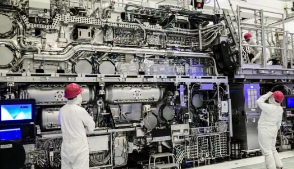
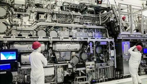
EUV (extreme ultraviolet lithography) is crucial for semiconductor manufacturing at scales of 5 nanometers and smaller, allowing more transistors to fit on a chip and increasing computing power.
And EUV equipment is expensive, costing over 40 billion yen ($273 million) per unit, making it a significant investment for suppliers of materials and equipment.
The U.S. has tightened restrictions on EUV-related exports to China amid growing strategic competition with China, slowing the return of research data to Japan. Having EUV equipment available at a domestic research facility will reduce this barrier, according to the report.
ASML Holding, based in the Netherlands, is the leading manufacturer of EUV lithography equipment. However, semiconductor production involves over 600 steps, requiring a broad range of specialized equipment and materials.
Japanese companies like Lasertec dominate the EUV inspection equipment market, and firms like JSR specialize in photosensitive materials for silicon wafer circuits.
Intel aims to strengthen ties with these Japanese suppliers through the new research center.