The original NMOS version of the MOS 6502, used in computers like the Commodore 64, the Apple II and the Nintendo Entertainment System (NES), is well-known for its illegal opcodes: Out of 256 possible opcodes, 151 are defined by the architecture, but many of the remaining 105 undefined opcodes do useful things.
Many articles have been written to test and document these, but I am not aware of any article that tries to explain where exactly they come from. I’ll do this here.
The Block Diagram
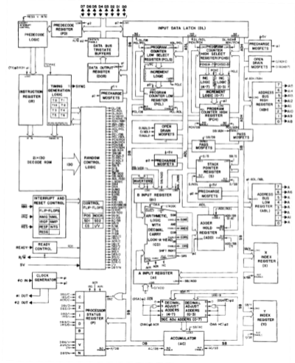
Every 6502 data sheet comes with a block diagram, but these are of no use, because they are oversimplified, partially incorrect, and don’t explain how instruction decoding works. The following more detailed diagram is a lot more useful:
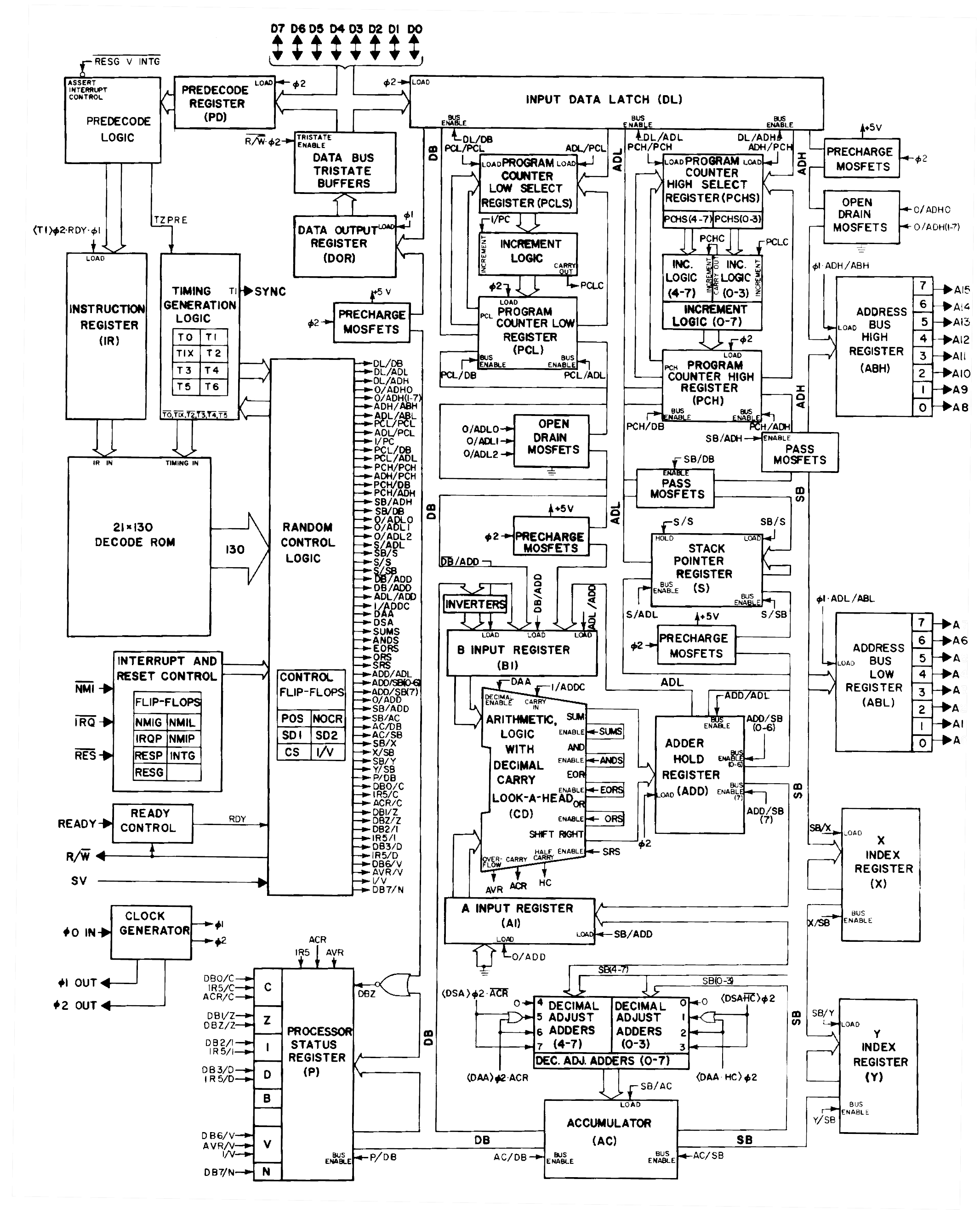
(Original from Apple II things)
The Decode ROM (PLA)
There is no need to understand the whole diagram. The important part is on the left: The instruction register, which holds the opcode, and the current clock cycle within the instruction (T0 to T6) get fed into a 130×21 bit decode ROM, i.e. a ROM with 130 lines of 21 bits each. On the die shot, this is the green area on the bottom.
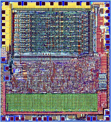
(Original from Molecular Expressions)
While other CPUs from the same era used microcode to interpret the instruction, the 6502 had this 130×21 bit PLA. All lines of the PLA compare the instruction and the current clock cycle, and if they match, the line fires. A little simplified, every line looks like this:
| ON bits | OFF bits | timing | |||||||||||||||||||
| 7 | 6 | 5 | 4 | 3 | 2 | 1 | 0 | 7 | 6 | 5 | 4 | 3 | 2 | 1 | 0 | T6 | T5 | T4 | T3 | T2 | T1 |
(See the diagrams at http://impulzus.sch.bme.hu/6502/ for details; partial English translation of the website here).
- “ON bits” specifies, which bits need to be set for this line to fire.
- “OFF bits” specifies, which bits need to be clear for this line to fire.
The opcode table of the 6502 is laid out in a way that you can find easy rules to generalize the effects of similar opcodes. For example, the branch opcodes are encoded like this:
%aab10000
where “aa” is the condition (00=N, 01=V, 10=C, 11=Z) and “b” decides whether the branch is taken on a set or a clear flag.
So the following line would fire on the first cycle of any branch:
| ON bits | OFF bits | timing | |||||||||||||||||||
| 7 | 6 | 5 | 4 | 3 | 2 | 1 | 0 | 7 | 6 | 5 | 4 | 3 | 2 | 1 | 0 | T6 | T5 | T4 | T3 | T2 | T1 |
| 0 | 0 | 0 | 1 | 0 | 0 | 0 | 0 | 0 | 0 | 0 | 0 | 1 | 1 | 1 | 1 | 0 | 0 | 0 | 0 | 0 | 1 |
From now on, let’s write it differently, so that it’s more readable:
| mask | cycle | description |
| XXX10000 | T1 | T1 of Bcc: fetch branch offset |
If a line fires, it outputs a “1”. The “Random Control Logic” that can seen in the diagram then AND/OR-combines some lines and feeds the result into various components of the CPU: In the case of a branch, this would result in fetching the branch offset, for example.
One line can fire for several opcodes that are similar in their encoding and thus their behavior: For example, “LDA abs”, “ORA abs” and “AND abs” all do the same thing (fetch the low byte of the address) in T1, so there can be a line that matches all these opcodes and causes a memory fetch and a PC increment. Also, multiple lines can fire at the same time for any given cycle within an instruction, which will have the combined effect of the single lines.
LDA and LDX becomes LAX
Now there are many undefined opcodes. The designers of the 6502 have not created any specific PLA lines for them, but since their opcodes are similar to well-defined opcodes, there might be lines that fire nevertheless.
Let’s take opcode $AF for example, which is “LAX absolute”. It loads a value from an absolute address in memory and stores it in A and X at the same time. This is somewhat the combination of opcodes $AD (LDA abs) and $AE (LDX abs).
The instructions “LDA/LDX/LDY abs” ($AC/$AD/$AE) consist of four cycles:
- The first cycle fetches the low byte of the address.
- The second cycle fetches the hgh byte of the address.
- The third cycle fetches the address from memory and stores it in A/X/Y.
- The fourth cycle fetches the next instruction.
Cycles T1, T2 and T4 are identical for all three of them, and they are encoded smilarly, so the following three PLA lines can be used to detect these instructions and signal the rest of the CPU to carry out the specific tasks:
| mask | cycle | description |
| 101011XX | T1 | T1 of $AC/$AD/$AE: fetch addr/lo |
| 101011XX | T2 | T2 of $AC/$AD/$AE: fetch addr/lo |
| 101011XX | T4 | T4 of $AC/$AD/$AE: fetch next opcode |
The mask %101011XX doesn’t only fire for $AC/$AD/$AE, but also for the undefined opcode $AF: So $AF (LAX) behaves the same as LDA/LDX/LDY in T1/T2/T4, i.e. it fetches a 16 bit address and in the end fetches the next opcode.
T3 differs in all three cases, so it has to be handled by one separate line per case:
| mask | cycle | description |
| 10101100 | T3 | T3 of $AC: read into Y |
| 101011X1 | T3 | T3 of $AD: read into A |
| 1010111X | T3 | T3 of $AE: read into X |
(Actually, the lines in the actual PLA might be less specific, i.e. contain more X bits, since there are similar instructions like “ORA absolute” that might share this line.)
The line for $AC is only true for the exact value of $AC, but the $AD and $AE lines have one “don’t care” bit each. The bitfield of $AF, which is %10101111, is true for both masks, so in T3 of $AF, both the $AD and the $AE lines fire.
In T3, LDA/LDX/LDY have in common that they all read from memory and put the result onto the internal “SB” bus. “LDA” also sets the “SB->AC” control line to “1”, which will make the accumulator read its value from SB. Likewise, LDX causes “SB->X” to be “1” and makes X to read from the SB bus, and LDY reads SB into the Y register.
Since both the LDA and the LDX lines fire, both the accumulator and the X register will be sent the command to load their values from the SB bus, so $AF is effectively an LAX: Load Accumulator and X.
The KIL Opcodes
There are many “KIL” opcodes, i.e. opcodes that stop the CPU, so that it can only recover using a RESET, and not even an IRQ or an NMI.
In order to understand this, let’s look at the different states an instruction can be in. After the instruction fetch, the CPU is in cycle T1. It will feed the opcode and the cycle number into the PLA and cause the rest of the CPU to carry out whatever has to be done in this cycle, according to the PLA. Then it will shift the T bitfield left by one, so the T2 line will be “1”, then line T3 and so on. There are seven T lines total, T1 to T7. At the end of each instruction, the PLA causes the T bitfield to reset, so that the next instruction starts with T1=1 again.
But what happens if T does not get reset? This can happen if in all seven states of T, no line fires that actually belongs to an instruction that ends at this cycle. T gets shifted left until state T7, in which another shift left will just shift the 1 bit out of T – all bits of T will be zero then, so no PLA line can fire any more.
All interrupt and NMI requests are always delayed until the current instruction is finished, i.e. until T gets reset. But since T never gets reset, all interrupts and NMIs are effectively disabled.
What’s next?
There are many illegal opcodes, some with very weird behavior, and some that have been documented as unstable. Studying all these can reveal many interesting details about the internal design of the 6502.