CDNA 4 is AMD’s latest compute oriented GPU architecture, and represents a modest update over CDNA 3. CDNA 4’s focus is primarily on boosting AMD’s matrix multiplication performance with lower precision data types. Those operations are important for machine learning workloads, which can often maintain acceptable accuracy with very low precision types. At the same time, CDNA 4 seeks to maintain AMD’s lead in more widely applicable vector operations.
To do so, CDNA 4 largely uses the same system level architecture as CDNA 3. It’s massive chiplet setup, with parallels to AMD’s successful use of chiplets for CPU products. Accelerator Compute Dies, or XCDs, contain CDNA Compute Units and serve a role analogous to Core Complex Dies (CCDs) on AMD’s CPU products. Eight XCDs sit atop four base dies, which implement 256 MB of memory side cache. AMD’s Infinity Fabric provides coherent memory access across the system, which can span multiple chips.
Compared to the CDNA 3 based MI300X, the CDNA 4 equipped MI355X slightly cuts down CU count per XCD, and disables more CUs to maintain yields. The resulting GPU is somewhat less wide, but makes up much of the gap with higher clock speeds. Compared to Nvidia’s B200, both MI355X and MI300 are larger GPUs with far more basic building blocks. Nvidia’s B200 does adopt a multi-die strategy, breaking from a long tradition of using monolithic designs. However, AMD’s chiplet setup is far more aggressive and seeks to replicate their scaling success with CPU designs with large compute GPUs.
CDNA 3 provided a huge vector throughput advantage over Nvidia’s H100, but faced a more complicated situation with machine learning workloads. Thanks to a mature software ecosystem and a heavy focus on matrix multiplication throughput (tensor cores), Nvidia could often get close (https://chipsandcheese.com/p/testing-amds-giant-mi300x) to the nominally far larger MI300X. AMD of course maintained massive wins if the H100 ran out of VRAM, but there was definitely room for improvement.
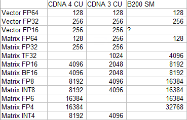
CDNA 4 rebalances its execution units to more closely target matrix multiplication with lower precision data types, which is precisely what machine learning workloads use. Per-CU matrix throughput doubles in many cases, with CDNA 4 CUs matching Nvidia’s B200 SMs in FP6. Elsewhere though, Nvidia continues to show a stronger emphasis on low precision matrix throughput. B200 SMs have twice as much per-clock throughput as a CDNA 4 CU across a range of 16-bit and 8-bit data types. AMD continues to rely on having a bigger, higher clocked GPU to maintain an overall throughput lead.

With vector operations and higher precision data types, AMD continues MI300X’s massive advantage. Each CDNA 4 CU continues to have 128 FP32 lanes, which deliver 256 FLOPS per cycle when counting FMA operations. MI355X’s lower CU count does lead to a slight reduction in vector performance compared to MI300X. But compared to Nvidia’s Blackwell, AMD’s higher core count and higher clock speeds let it maintain a huge vector throughput lead. Thus AMD’s CDNA line continues to look very good for high performance compute workloads.
Nvidia’s focus on machine learning and matrix operations keeps them very competitive in that category, despite having fewer SMs running at lower clocks. AMD’s giant MI355X holds a lead across many data types, but the gap between AMD and Nvidia’s largest GPUs isn’t nearly as big as with vector compute.
GPUs provide a software managed scratchpad local to a group of threads, typically ones running on the same core. AMD GPUs use a Local Data Share, or LDS, for that purpose. Nvidia calls their analogous structure Shared Memory. CDNA 3 had a 64 KB LDS, carrying forward a similar design from AMD GCN GPUs going back to 2012. That LDS had 32 2 KB banks, each 32 bits wide, providing up to 128 bytes per cycle in the absence of bank conflicts.
CDNA 4 increases the LDS capacity to 160 KB and doubles read bandwidth to 256 bytes per clock. GPUs natively operate on 32 bit elements, and it would be reasonable to assume AMD doubled bandwidth by doubling bank count. If so, each bank may now have 2.5 KB of capacity. Another possibility would be increasing bank count to 80 while keeping bank size at 2 KB, but that’s less likely because it would complicate bank selection. A 64-banked LDS could naturally serve a 64-wide wavefront access with each bank serving a lane. Furthermore, a power-of-two bank count would allow simple bank selection via a subset of address bits.
The larger LDS lets software keep more data close to the execution units. Kernels can allocate more LDS capacity without worrying about lower occupancy due to LDS capacity constraints. For example, a kernel that allocates 16 KB of LDS could run four workgroups on a CDNA 3 CU. On CDNA 4, that would increase to ten workgroups.
Software has to explicitly move data into the LDS to take advantage of it, which can introduce overhead compared to using a hardware-managed cache. CDNA 3 had GLOBAL_LOAD_LDS instructions that let kernels copy data into the LDS without going through the vector register file, CDNA 4 augments GLOBAL_LOAD_LDS to support moving up to 128 bits per lane, versus 32 bits per lane on CDNA 3. That is, the GLOBAL_LOAD_LDS instruction can accept sizes of 1, 2, 4, 12, or 16 DWORDS (32-bit elements), versus just 1, 2, or 4 on CDNA 3.1
CDNA 4 also introduces read-with-transpose LDS instructions. Matrix multiplication involves multiplying elements of a row in one matrix with corresponding elements in a second matrix’s column. Often that creates inefficient memory access patterns, for at least one matrix, depending on whether data is laid out in row-major or column-major order. Transposing a matrix turns the awkward row-to-column operation into a more natural row-to-row one. Handling transposition at the LDS is also natural for AMD’s architecture, because the LDS already has a crossbar that can map bank outputs to lanes (swizzle).
Even with its LDS capacity increase, AMD continues to have less data storage within its GPU cores compared to Nvidia. Blackwell’s SMs have a 256 KB block of storage partitioned for use as both L1 cache and Shared Memory. Up to 228 KB can be allocated for use as Shared Memory. With a 164 KB Shared Memory allocation, which is close to matching AMD’s 160 KB LDS, Nvidia would still have 92 KB available for L1 caching. CDNA 4, like CDNA 3, has a 32 KB L1 vector cache per CU. Thus a Blackwell SM can have more software managed storage while still having a larger L1 cache than a CDNA 4 CU. Of course, AMD’s higher CU count means there’s 40 MB of LDS capacity across the GPU, while Nvidia only has ~33 MB of Shared Memory across B200 with the largest 228 KB Shared Memory allocation.
To feed the massive arrays of Compute Units, MI355X largely uses the same system level architecture as MI300X. MI355X does see a few enhancements though. The L2 caches can “writeback dirty data and retain a copy of the line”. “Dirty” refers to data that has been modified in a write-back cache, but hasn’t been propagated to lower levels in the memory subsystem. When a dirty line is evicted to make room for newer data, its contents are written back to the next level of cache, or DRAM if it’s the last level cache.
AMD may be seeking to opportunistically use write bandwidth when the memory subsystem is under low load, smoothing out spikes in bandwidth demand caused by cache fill requests accompanied by writebacks. Or, AMD could be doing something special to let the L2 transition a line to clean state if written data is likely to be read by other threads across the system, but isn’t expected to be modified again anytime soon.
MI355X’s DRAM subsystem has been upgraded to use HBM3E, providing a substantial bandwidth and capacity upgrade over its predecessor. It also maintains AMD’s lead over its Nvidia competition. Nvidia also uses HBM3E with the B200, which also appears to have eight HBM3E stacks. However, the B200 tops out at 180 GB of capacity and 7.7 TB/s of bandwidth, compared to 288 GB at 8 TB/s on the MI355X. The MI300X could have a substantial advantage over Nvidia’s older H100 when the H100 ran out of DRAM capacity, and AMD is likely looking to retain that advantage.
Higher bandwidth from HBM3E also helps bring up MI355X’s compute-to-bandwidth ratio. MI300X had ~0.03 bytes of DRAM bandwidth per FP32 FLOP, which increases to 0.05 on MI355X. Blackwell for comparison has ~0.10 bytes of DRAM bandwidth per FP32 FLOP. While Nvidia has increased last level cache capacity on Blackwell, AMD continues to lean more heavily on big caches, while Nvidia relies more on DRAM bandwidth.
CDNA 2 and CDNA 3 made sweeping changes compared to their predecessors. CDNA 4’s changes are more muted. Much like going from Zen 3 to Zen 4, MI355X retains a similar chiplet arrangement with compute and IO chiplets swapped out for improved versions. Rather than changing up their grand strategy, AMD spent their time tuning CDNA 3. Fewer, higher clocked CUs are easier to utilize, and increased memory bandwidth can help utilization too. Higher matrix multiplication throughput also helps AMD take on Nvidia for machine learning workloads.
In some ways, AMD’s approach with this generation has parallels to Nvidia’s. Blackwell SMs are basically identical to Hopper’s from a vector execution perspective, with improvements focused on the matrix side. Nvidia likely felt they had a winning formula, as their past few GPU generations have undoubtedly been successful. AMD may have found a winning formula with CDNA 3 as well. MI300A, MI300X’s iGPU cousin, powers the highest ranking supercomputer on TOP500’s June list.4 Building on success can be a safe and rewarding strategy, and CDNA 4 may be doing just that.
If you like the content then consider heading over to the Patreon or PayPal if you want to toss a few bucks to Chips and Cheese. Also consider joining the Discord.
https://github.com/llvm/llvm-project/blob/main/clang/test/CodeGenOpenCL/builtins-amdgcn-gfx950.cl - b96 and b128 (96-bit and 128-bit) global_load_lds sizes
https://github.com/llvm/llvm-project/blob/84ff1bda2977e580265997ad2d4c47b18cd3bf9f/mlir/include/mlir/Dialect/LLVMIR/ROCDLOps.td#L426C1-L426C50 - LDS transpose intrinsics
https://docs.nvidia.com/cuda/blackwell-tuning-guide/index.html
https://www.reddit.com/r/hardware/comments/1kj38r1/battle_of_the_giants_8x_nvidia_blackwell_b200/ - reports 148 Compute Units via OpenCL for B200. Nvidia usually reports SMs for the Compute Unit count