Hot on the heels of our 10K word deep dive on TPUs, Amazon launched Trainium3 (Trn3) general availability and announced Trainium4 (Trn4) at its annual AWS re:Invent. Amazon has had the longest and broadest history of custom silicon in the datacenter. While they were behind in AI for quite some time, they are rapidly progressing to be competitive. Last year we detailed Amazon’s ramp of its Trainium2 (Trn2) accelerators aimed at internal Bedrock workloads and Anthropic’s training/inference needs.
Since then, through our datacenter model and accelerator model, we detailed the huge ramp that led to our blockbuster call that AWS would accelerate on revenue.
Today, we are publishing our next technical bible on the step-function improvement that is the Trainium3 chip, microarchitecture, system and rack architecture, scale up, profilers, software platform, and datacenters ramps. This is the most detailed piece we've written on an accelerator and its hardware/software, on desktop there is a table of contents that makes it possible to review specific sections.
With Trainium3, AWS remains laser-focused on optimizing performance per total cost of ownership (perf per TCO). Their hardware North Star is simple: deliver the fastest time to market at the lowest TCO. Rather than committing to any single architectural design, AWS maximizes operational flexibility. This extends from their work with multiple partners on the custom silicon side to the management of their own supply chain to multi-sourcing multiple component vendors.
On the systems and networking front, AWS is following an “Amazon Basics” approach that optimizes for perf per TCO. Design choices such as whether to use a 12.8T, 25.6T or a 51.2T bandwidth scale-out switch or to select liquid vs air cooling are merely a means to an end to provide the best TCO for the given client and the given datacenter.
For the scale-up network, while Trn2 only supports a 4x4x4 3D Torus mesh scaleup topology, Trainium3 adds a unique switched fabric that is somewhat similar to the GB200 NVL36x2 topology with a few key differences. This switched fabric was added because a switched scaleup topology has better absolute performance and perf per TCO for frontier Mixture-of-Experts (MoE) model architectures.
Even for the switches used in this scale-up architecture, AWS has decided to not decide: they will go with three different scale-up switch solutions over the lifecycle of Trainium3, starting with a 160 lane, 20 port PCIe switch for fast time to market due to the limited availability today of high lane & port count PCIe switches, later switching to 320 Lane PCIe switches and ultimately a larger UALink to pivot towards best performance.
On the software front, AWS’s North Star expands and opens their software stack to target the masses, moving beyond just optimizing perf per TCO for internal Bedrock workloads (ie DeepSeek/Qwen/etc which run a private fork of vLLM v1) and for Anthropic’s training and inference workloads (which runs a custom inference engine and all custom NKI kernels).
In fact, they are conducting a massive, multi-phase shift in software strategy. Phase 1 is releasing and open sourcing a new native PyTorch backend. They will also be open sourcing the compiler for their kernel language called “NKI” (Neuron Kernal Interface) and their kernel and communication libraries matmul and ML ops (analogous to NCCL, cuBLAS, cuDNN, Aten Ops). Phase 2 consists of open sourcing their XLA graph compiler and JAX software stack.
By open sourcing most of their software stack, AWS will help broaden adoption and kick-start an open developer ecosystem. We believe the CUDA Moat isn’t constructed by the Nvidia engineers that built the castle, but by the millions of external developers that dig the moat around that castle by contributing to the CUDA ecosystem. AWS has internalized this and is pursuing the exact same strategy.
Trainium3 will only have Day 0 support for Logical NeuronCore (LNC) = 1 or LNC = 2. LNC = 1 or LNC = 2 is what ultra-advanced, elite L337 kernel engineers at Amazon/Anthropic want, but LNC=8 is what the wider ML research scientist community prefers before widely adopting Trainium. Unfortunately, AWS does not plan on supporting LNC=8 until mid-2026. We will expand much more on what LNC is and why the different modes are critical for research scientist adoption further down.
Trainium3’s go-to-market opens yet another front Jensen must now contend with in addition to the other two battle theatres facing the extremely strong perf per TCO Google’s TPUv7 as well as a resurgent AMD’s MI450X UALoE72 with potentially strong perf per TCO (especially after the “equity rebate” OpenAI gets to own up to 10% of AMD shares).
We still believe Nvidia will stay King of the Jungle as long as they continue to keep accelerating their pace of development and move at the speed of light. Jensen needs to ACCELERATE even faster than he has over the past 4 months. In the same way that Intel stayed complacent in the CPU while others like AMD and ARM raced ahead, if Nvidia stays complacent they will lose their pole position even more rapidly.
Today, we will discuss the two Trainium3 rack SKUs that support switched scale-up racks:
We will start by briefly reviewing the Trn2 architecture and explaining the changes introduced with Trainium3. The first half of the article will focus on the various Trainium3 rack SKUs’ specifications, silicon design, rack architecture, bill of materials (BoM) and power budget before we turn to the scale-up and scale-out network architecture. In the second half of this article, we will focus on discussing the Trainium3 Microarchitecture and expand further on Amazon’s software strategy. We will conclude with a discussion on Amazon and Anthropic’s AI Datacenters before tying everything together with a Total Cost of Ownership (TCO) and Perf per TCO analysis.
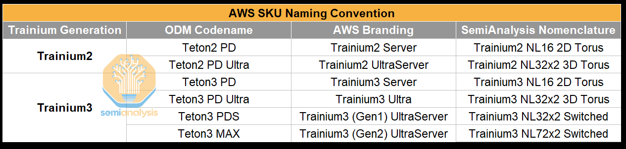
In total, there are four different server SKUs between Trainium2 and Trainium3 that the supply chain often refers to by their codenames, which are different than AWS’s branding.
Readers probably will find it confusing untangling the various generation and rack form factor combinations, switching back and forth between AWS’s branding and the codenames that the ODMs/Supply Chain use. Our plea to AWS: whoever is in charge of product marketing and naming needs to stop with these confusing names. It would be ideal if they could follow along with Nvidia and AMD with a nomenclature whereby the second half of the product name denotes the scaleup technology and the world size i.e. the NVL72 in GB200 NVL72 referring to NVLink with a 72 GPU world size.
In the table below we aim to unconfuse our readers with a Rosetta stone for the various naming conventions different groups have been using:

Trainium3 delivers several notable generation on generation upgrades when it comes to specifications.
OCP MXFP8 FLOPs throughput is doubled, and OCP MXFP4 support is added but at the same performance as OCP MXFP8. Performance for higher precision number formats like FP16 and FP32 interestingly remain the same as for Trn2. In the microarchitecture section, we will describe the implications of these tradeoffs.
The HBM3E is upgraded to 12-high for Trainium3 which brings memory capacity to 144GB per chip. Despite maintaining 4 stacks of HBM3E, AWS has achieved a 70% increase in memory bandwidth by going from below average pin speeds of 5.7Gbps for Trn2 to 9.6Gbps for Trn3, which is the highest HBM3E pin speeds we’ve seen yet. In fact, the 5.7Gbps pin speed that was used in Trn2 is more in line with HBM3 speeds, but it is still classified as HBM3E because it uses 24Gb dies to provide 24GB per stack in an 8-layer stack. The speed deficiency was due to using memory supplied by Samsung, whose HBM3E is notably sub-par compared to that of Hynix or Micron. For the HBM used in Trainium3, AWS is switching to Hynix and Micron to achieve much faster speeds. For per vendor share of HBM by accelerator, use our accelerator model.
The scale-up bandwidth per Trainium3 chip is doubled vs Trn2 by moving to PCIe Gen 6 which offers 64Gbps per lane (uni-directional) vs the 32Gbps per lane offered by PCIe Gen 5. Trainium3 uses 144 active lanes of PCIe for scale up, which on Gen6 means each Trainium3 supports 1.2 TB/s (uni-directional) of scale-up bandwidth per chip.
Scale-out bandwidth support is doubled to a maximum of 400 Gb/s, but most Trainium3 racks produced will stick with the 200Gb/s per XPU scale-out speed that was used for Trn2.
For Trainium4, Amazon will use 8 stacks of HBM4, achieving 4x the memory bandwidth and 2x the capacity compared to Trainium3.
Zooming out to the rack solution level, AWS announced at re:Invent the Trainium3 (Gen1) UltraServer and the Trainium3 (Gen2) UltraServer, which correspond to the Trainium3 NL32x2 Switched and Trainium3 NL72x2 Switched names respectively. The key difference between the Trainium3 NL32x2 Switched and the Trainium3 NL72x2 Switched is in the scale-up networking topology and rack architecture – this section will cover how topology and architecture differs between the two SKUs and discuss the AI workloads that each architecture is the most suitable and optimized for.
Let’s start by going through the physical layout of each server type. The table below displays key specifications for each rack-scale SKU:
While Trainium2 will only be available in the first two rack SKU types – namely the Trn2 NL16 2D Torus and Trn2 NL32x2 2D Torus servers, Trainium3 will be offered in all four rack SKU types, with the majority of Trainium3 delivered in the Trainium3 NL32x2 Switched SKU in 2026. We expect that most of the Trainium3 to be deployed in the Trainium3 NL32x2 Switched and Trainium3 NL72x2 Switched SKUs during its lifecycle.
Trainium3’s compute moves to the N3P node from the N5 node that is used for Trn2. Trainium3 will be one of the first adopters of N3P along with Vera Rubin and the MI450X’s Active Interposer Die (AID). There have been some issues associated with N3P leakage that need to be fixed, which can push timelines out. We have detailed this and its impact in the accelerator model.
We see TSMC’s N3P as the “HPC dial” on the 3nm platform, a small but meaningful step beyond N3E for extra frequency or lower power without new design rules. Public data suggests N3P keeps N3E’s rules and IP but adds about 5% higher speed at iso-leakage, or 5-10% lower power at iso-frequency, plus roughly 4% more effective density on mixed logic/SRAM/analog designs. This is exactly the type of incremental, low-friction gain hyperscalers want for giant AI ASICs.
Trainium3 is a good example of the kind of product that makes sense to build on this node. Trainium3 is emblematic of why custom accelerators will soak up 3 nm HPC capacity: dense matrix engines, fat SRAM slices, and very long on-die interconnects that benefit from every small reduction in device delay and leakage.
Under the hood, N3P is less a single breakthrough than many stacked Design-Technology Co-Optimization (DTCO tweaks). N3 generation FinFlex libraries let designers mix wider and narrower fins inside a block, trading off drive strength versus area and leakage at fine granularity. TSMC has also refined liners and barrier processes in the lower metal stack of N3P that reduce line and via resistance compared with earlier 3nm incarnations. Together, these changes claw back enough margin to support higher clocks or lower Vmin on long global paths.
The challenge is that N3P does this while pushing interconnect scaling and patterning almost as far as current EUV tools allow. Minimum metal pitches in the low 20s of nanometers, high aspect ratio vias, and tighter optical shrinks all amplify BEOL variability and RC. Issues like via profile control, under-etch, and dielectric damage become first order timing problems. For TSMC, that means more fragile process windows, more sophisticated in-line monitoring, and heavier use of DTCO feedback loops to keep design rules aligned with what the line can print at scale. We currently see a slower than expected improvement in defect density of N3P, which is causing chip designers to either re-spin for yield or to wait in the queue for process improvements.
Readers who decipher die markings will see that the package shot above is just Trn2, and this is what we’ve used, as its package layout is exactly the same as Trainium3. The package is composed of two CoWoS-R assemblies, rather than one large interposer. The two compute dies interface with each other through the substrate.
Trainium3 will continue to utilize TSMC’s CoWoS-R, the platform that pushes power and latency limits while staying cost competitive. Instead of a full silicon interposer, Trainium3 follows its predecessor Trainium2 to use an organic thin-film interposer with six layers of copper RDLs on polymer, spanning a reticle-scale footprint at much lower cost and better mechanical compliance than silicon interposers. It still supports fine wiring and micro-bump pitches of a few tens of micrometers between dies and the interposer, which is critical for dense chiplet fabrics and HBM interfaces. Underneath sits a high layer count ABF substrate of twenty build-up layers that fans out power and XSR signals to 130 to 150 micrometer C4 bumps at the module boundary, where the MCM connects to the board.
Multiple RDL layers above six layers on CoWoS-R are a deliberate compromise rather than a hard limit. Purely organic interposers are cheap and compliant but they eventually run out of beachfront when we try to integrate more lanes at 32 gigabits per second or more. IPDs (integrated passive devices) close that gap by dropping small silicon passive components into the organic landscape only where necessary. These thousands of IPDs in each RDL interposer enable sub-micron wiring density, very fine micro-bump pitches, and strong decoupling under the noisiest parts of the chip such as HBM PHY rings and core fabrics.
The chip’s front end is designed by Annapurna with the PCIe SerDes licensed from Synopsys. Alchip does the back end physical design and package design. We believe there may be some interface IP inherited from Marvell-designed Trainium2 in Trainium3, but it’s not meaningful in terms of content. Marvell also has package design at other 3rd party vendors.
Interestingly, there are two tapeouts with one mask set owned by Alchip (called “Anita”), and another set owned by Annapurna directly (“Mariana”). With the Anita variant, Alchip procures chip components from TSMC directly, and Annapurna procures chip components directly for Mariana. The majority of volumes will be for Mariana. While Alchip had similar levels of design involvement for Mariana, the revenue they will see from Mariana should be lower than for Anita. Amazon and Annapurna are heavily cost focused and drive their suppliers hard. Compared to Broadcom’s ASIC deals, the Trainium projects have much less profit pool available to the chip design partners Alchip and Marvell. When it comes to performance per TCO – Annapurna places greater emphasis on driving down the TCO denominator.
Marvell ends up being the big loser from this. While they designed Trainium2, they lost the design bakeoff with Alchip for this generation. Marvell’s Trainium3 version was a chiplet based design, with the I/O being put onto a separate chiplet, instead of on a monolithic die with the compute as is the case with Trainium2 and what will be Trainium3.
Marvell lost this socket due to poor execution for Trainium2. The development timeline took far too long. Marvell had problems designing the RDL interposer for the package as well, and Alchip had to step in to help deliver something workable.
For Trainium4, multiple design houses will be involved across two different tracks based on different scale-up protocols. We first detailed the UALink / NVLink split for Trainium 4 in the accelerator model 7 months ago in May. Alchip just as in Trainium3 leads the backend design for both tracks.
There will likely be a significant timing gap between Nvidia’s VR NVL144, and NVLink Fusion products like Trainium4. For the NVLink fusion track, timelines may slip even further, as the fusion chiplet introduces additional integration and validation requirements & most of the NVIDA mixed signal engineers will be focusing their attention on Nvidia VR NVL144 new product introduction.
While Trainium4 with NVLink fusion may not arrive soon, we believe AWS secured favorable commercial terms and is unlikely to be paying Nvidia’s typical ~75 % gross margins. Nvidia has strong strategic incentives to enable interoperability with Trainium4, since allowing AWS to use NVLink helps preserve Nvidia’s system-level lock-in. As a result, Nvidia is likely to offer more attractive pricing than it would under its standard gross margin structure.
Unlike VR NVL144, which is limited to a fixed 72-package NVLink domain, Trainium4 can extend NVLink scale-up via cross rack AECs, enabling much larger 144+ coherent domains. NVLink 6 uses 400G bidirectional SerDes, allowing 200G RX and 200G TX simultaneously on the same wire at the same time. This 400G BiDi signaling already pushes copper to its practical limits, and although some vendors may attempt a half-generation step to 600G BiDi.
Trainium2 NL16 2D Torus and Trainium2 NL64 3D Torus SKUs are branded as the Trainium2 Server and the Trainium2 UltraServer respectively and were announced at re:Invent 2024. We covered both architectures in our Trainium2 deep dive:
To briefly revisit the Trainium2 SKUs - the key difference between the Trainium2 NL16 2D Torus and Trainium2 NL64 3D Torus SKUs is the scale-up world size. While Trainium2 NL16 2D Torus occupies half a server rack for the entire scale-up world size, with that world size containing 16 Trainium2s in a 4x4 mesh 2D torus, Trainium2 NL32x2 3D Torus connects four Trainium2 NL16 2D Torus half racks together – taking up two racks in total. The four Trainium2 NL16 2D Torus half rack servers are connected using AECs to create a scale up world size of 64 Trainium2s in an 4x4x4 3D Torus.
Do note that in the above diagram, that the Trainium2 NL16 2D Torus diagram represents a full rack but includes two scale-up worlds within the rack diagrammed.
As mentioned, Trainium2 is only offered in the NL16 2D Torus and NL32x2 3D Torus rack SKUs, which feature the 2D and 3D Torus topology respectively, and there is no switched topology offering. Most of the Trainium2 deployment will be of the Trainium2 NL64 3D Torus form factor as Anthropic’s Project Rainier is driving most of the demand, hence production will follow their preference for the NL64 3D Torus. This is due to Anthropic’s inferencing models requiring a larger scale up topology.
When Nvidia introduced the Oberon architecture (GB200 NVL72) with an all-to-all scale up topology and a scale up world size of 72 chips, many ASIC and GPU manufacturers pivoted their future rack design roadmaps to emulate Nvidia’s Oberon architecture. While AMD was the first to announce an Oberon-like architecture with the MI400 Helios rack, AWS will be the first outside of Nvidia to actually ship and deploy a similar all-to-all switched scale-up architecture with the Trainium3 in the Trainium3 NL32x2 Switched and Trainium3 NL72x2 Switched form factor. AMD’s first rack scale design, MI450X UALoE72 will arrive a year later than Trainium3’s rack scale design and is targeting end of year. Meta will ship their first switched architecture before AMD’s MI450X as well. We explain later in the “3D Torus vs Switched” section of this article why the switched scale up architecture is preferred over a torus architecture.
The Trainium3 UltraServer showed at re:Invent maps to the Trainium3 NL72x2 Switched rack SKU, but the Trainium3 NL72x2 Switched is just one of two flavors of the Trainium3 all-to-all switched racks – the other is known as the Trainium3 NL32x2 Switched. Like the Trainium3 NL72x2 Switched, the Trainium3 NL32x2 Switched is also all-to-all switched, but it differs from the Trainium3 NL72x2 Switched in that the Trainium3 NL32x2 Switched is air cooled, and as such offers a smaller scale-up world size and has a lower power density.
The Trainium3 NL32x2 Switched has a very similar rack layout to the Trainium NL32x2 3D Torus. Both have 16 JBOG (Just a Bunch of GPUs) Trays and two host CPU trays per rack. There are two Trainium3 accelerators per JBOG Tray, so there is a total of 32 Trainium3 chips per rack. A full Trainium3 NL32x2 Switched scale-up world is made up of two racks of 32 Trainium3 chips each to build up a total world size of 64 Trainium3s.
The key difference between the Trainium NL32x2 3D Torus and the Trainium NL32x2 Switched is the addition of the scale-up NeuronLink switch trays in the middle of the rack for the Trainium NL32x2 Switched that enables the all-to-all switched network. The NeuronLink switch trays are placed in the middle of the rack for the same reason as the NVLink switch trays are placed in the middle of Nvidia’s Oberon rack, to minimize the distance of the longest SerDes reach between the accelerator and the scale up switch. For the Trainium NL32x2 Switched, the CPU trays, power shelves, Battery Backup Unit (BBU) trays and Top of Rack (ToR) Switches are also moved from being always at the top of each respective 8 JBOG tray groups to being at the top and the bottom of the rack to reduce the distances between the 16 JBOG trays and the four NeuronLink switch trays. There will also be designs with five NeuronLink switch trays such that they can hot swap switch trays without downtime. This contrasts with Nvidia’s GB200/300 NVL72/VR NVL144, where operators must first drain all the workloads from the rack before swapping switch trays. Amazon’s philosophy is always centered around field serviceability and reliability due to their intimate role in deploying and managing. Nvidia chases performance at the cost of these other concerns because that’s what they sell.
The other major differences lie in the NeuronLink topology and related connectivity components. Trainium NL32x2 Switched will connect between two racks with cross rack AECs from one chip in Rack A directly to another chip in Rack B. We will discuss the scale-up network in greater detail later in the article.
The JBOG tray of the Trainium3 NL32x2 Switched will be very similar to that of the Trainium NL32x2 3D Torus. There will be two Trainium3 chips per JBOG. PCIe 6.0 based connectivity is used for the Trainium3 NL32x2 Switched – an upgrade vs the Trainium2 NL16 2D Torus and Trainium2 NL32x2 3D Torus JBOG which used PCIe 5.0 based connectivity. As a result of this, PCB materials will have to be upgraded from M8 grade copper clad laminate (CCL) (specifically, low DK2 glass fiber cloth + HVLP2 copper foil) to M8.5 grade CCL (Low DK2 glass fiber cloth + HVLP4 copper foil).
All Trainium racks thus far have adopted a cableless design philosophy to increase assembly efficiency, and so all the signals are transmitted through PCB traces. Signal loss is far higher when traveling over PCB than when traveling over flyover cable, hence four PCIe 6.0 x16 retimers must be placed in the middle of the JBOG board to recondition the signal that travels over PCB between the front I/O ports and the two Trainium3 packages.
NICs for the Trainium3s are also found within the JBOG tray. For EFAv4, AWS’s backend network, there are two NIC configurations available for the Trainium3 NL32x2 Switched:
Option 1: One Nitro-v6 (2*200G) 400Gbps NIC module per JBOG tray of two Trainium3 chips: 200Gbps of EFA bandwidth per Trainium3
Option 2: Two Nitro-v6 (2*200G) 400Gbps Nitro NIC modules per JBOG tray of two Trainium3 chips: 400Gbps of EFA bandwidth per Trainium3.
The vast majority of Trainium3 based servers will use Option 1 – One Nitro-v6 400G NIC per two Trainium3 chips which equals to 200Gbps of scale-out bandwidth per Trainium3 chip. AWS believes that even for the largest production inferencing models today, 200Gbps per GPU is enough to overlap the KV cache transfer between prefill instances and decode instances. For training, the AWS philosophy is that small companies with elite programmers like those from Anthropic will use Pipeline Parallelism (PP) to reduce network volume and not just rely on FSDP/TP/Ctx Parallel/DP. It is important to remember, however, that Pipeline Parallelism is absolutely necessary for large scale training but a pain in the ass to maintain and debug codebases with PP.
For ENA, AWS’s frontend network, there is a dedicated Nitro-v6 (2*200) 400Gbps NIC module in the CPU tray. To connect each JBOG tray to the CPU tray, a dedicated PCIe 6.0 x16 DAC cable (128GByte/s uni-di) runs along the front of the server. The Trainium2 NL16 2D Torus connects the CPU trays and JBOG trays in the same fashion.
The CPU tray layout of Trainium3 NL32x2 Switched will be very similar to that of Trainium2 NL16 2D Torus, and is explained in the Trainium2 article.
The Trainium3 NL32x2 Switched is the time to market SKU for Trainium3 that supports a switched scale-up architecture. As it is an air-cooled rack, rack power density remains low. It can be thought of as the same power density profile as the Trainium3 NL32x2 3D Torus with the main difference simply being the addition of scale-up switch trays. Trainium3 NL32x2 Switched is also the only SKU with a switched scale-up architecture that can be deployed in datacenters that are not liquid cooled ready.
The use of air cooling provides a time to market advantage over other competitors’ liquid cooled scale-up switched accelerators since liquid cooled data center readiness is a key bottleneck of deployment currently. When operators try to force liquid cooled racks into an air-cooled datacenter, they must use an inefficient Liquid to Air sidecar. As such, we expect the majority of the Trainium3 chips deployed in 2026 to be in the form of the Trainium3 NL32x2 Switched SKU.
Both the Trainium3 NL32x2 Switched and Trainium3 NL72x2 Switched use an all-to-all switched architecture, but the Trainium3 NL72x2 Switched is the rack architecture that is most comparable to Nvidia’s GB200 NVL72 Oberon architecture. Other than both Oberon and Trainium3 NL72x2 Switched using liquid cooling, Trainium3 NL72x2 Switched integrates the CPU into the compute trays just like Nvidia does with Grace and Vera on the same compute tray as the GPUs. By comparison, Trainium NL32x2 Switched still uses a disaggregated CPU node. Like Oberon, Trainium NL72x2 Switched uses cold plates for liquid cooling of the Trainium3 accelerators and the Graviton 4 CPUs. The big difference of Trainium NL72x2 Switched from the Oberon architecture is the use of cross-rack connectivity to increase the scale up world size to span over two racks.
The Trainium3 NL72x2 Switched uses two racks to achieve a world size of 144 XPUs, and each rack houses 18 compute trays and 10 NeuronLink switch trays in the middle. With each compute tray housing four Trainium3 and one Graviton4 CPU, there are a total of 144 Trainium3s and 36 Graviton 4s across two racks making up the Trainium3 NL72x2 Switched world size. Just like Trainium3 NL32x2 Switched, Trainium3 NL72x2 Switched uses busbar to deliver power. The backplane utilizes a hybrid of connectors from both TE and Amphenol, for which we have the split in the networking model.
The higher compute and power density of the Trainium3 NL72x2 Switched starts from the compute tray, with each compute tray containing four Trainium3 chips. Trainium3 NL72x2 Switched connectivity is also mostly based on PCIe 6.0, therefore the PCB materials are the same as used for the Trainium3 NL32x2 Switched mentioned above. There are six PCIe 6.0 x16 retimers used to increase signal reach connecting between individual Trainium3 chips and the front I/O ports. Note that due to their cableless design to increase manufacturing speed, their time to market design includes a few inexpensive retimers that are designed in to de-risk the design. After a successful initial production deployment, AWS can look into optimizing the design and can potentially remove some of the retimers.
As discussed above, the main difference between the Trainium3 NL32x2 Switched and the Trainium3 NL72x2 Switched is in the cooling, where the Trainium3 NL72x2 Switched adopts liquid cooling vs Trainium3 NL32x2 Switched’s air cooling. Liquid cooling is used to cool the Trainium3 modules, the NeuronLinkv4 x32 lanes PCIe 6.0 switch, and the Graviton4 CPU. The rest of the items in the compute tray, the PCIe 6.0 x16 retimers, Nitro-v6 NICs, PCIe 6.0 x16 AEC cage, DIMMs, and 2x8TB local NVMe drives – are air-cooled using fans.
Turning to the host CPU, Graviton4 will be the only time to market CPU option for Trainium3 NL72x2 Switched. The CPU can be upgraded later to the next generation of Graviton during the Trainium3’s lifecycle. In theory, x86 CPUs are also supported as these can also interface with other components via PCIe, but we don’t believe that they will plan to have an x86 Trainium3 NL72x2 Switched SKU and will only offer an x86 Trainium NL32x2 Switched SKU. Because Trainium3 uses PCIe 6.0 and Graviton4 uses PCIe 5.0, two PCIe gearboxes must be placed next to the CPU to convert from PCIe 6.0 to PCIE 5.0 for communication between the CPU and GPUs. For CPU memory, 12 DDR5 DIMM slots are placed next to the CPU with DDR5 DIMM modules of 64GB and 128GB capacities to be used for the mainstream SKU. Two 8TB local NVMe drives per compute tray will be used for local storage.
Trainium3 NL72x2 Switched will have the same scale-out networking configuration as Trainium3 NL32x2 Switched, namely a choice between 400G or 200G scale-out bandwidth per Trainium3 chip:
Option 1: Two Nitro-V6 (2*200G) 400Gbps NIC module per JBOG tray of four Trainium3 chips: 200Gbps of EFA bandwidth per Trainium3
Option 2: Four Nitro-V6 (2*200G) 400Gbps Nitro NIC modules per JBOG tray of four Trainium3 chips: 400Gbps of EFA bandwidth per Trainium3.
Like the Trainium3 NL32x2 Switched, the vast majority of Trainium3 NL72x2 volume will be Option 1: One Nitro-v6 400G NIC per two Trainium3 chips which equals 200Gbps of scale-out bandwidth per Trainium3 chip.
The difference though is that for the Trainium3 NL72x2 Switched, the host CPUs are now located on the Compute Tray, and the CPU dedicated Nitro-V6 (2*200) 400Gbps NIC module is also located in the tray. Moreover, with PCIe switches, the CPU can also talk to the outside world using the Trainium3 dedicated NICs.
Trainium3 NL72x2 Switched is AWS’s answer to Nvidia’s Oberon rack architecture. The Trainium3 NL72x2 Switched architecture has much higher power density than its predecessor. Due to the high power density and need for liquid cooling ready datacenters, we expect some volume of Trainium3 to be deployed in the Trainium3 NL72x2 Switched SKU, but majority of the volume will still go toward Trainium3 NL32x2 Switched. After understanding the rack layout and compute tray layout/topology, it is time to dive into the real secret sauce that makes Trainium3 NL32x2 Switched and Trainium3 NL72x2 Switched stand out, the switched scale-up network topology.
Before we describe the exact topology of the new switched scale-up network – let’s first explain why AWS has chosen to pivot from a 2D/3D Torus into a switched architecture. The NeuronLinkv3 scale up topology for the Trainium2 NL26 2D Torus and Trainium2 NL32x2 3D Torus Servers is a 2D mesh Torus and 3D mesh Torus respectively (as the names would suggest!). However, keeping a Torus topology is not optimized for frontier Mixture of Experts (MoE) models which require all-to-all collectives. In contrast, dense models do not make extensive use of all-to-all collectives, meaning that a switched fabric does not have much of a perf advantage when used with dense models, while having higher TCO.
With a 3D Torus architecture, because of the oversubscription between chips within the scale-up domain, as message sizes grow from 16KB to 1MB (i.e. as you increase batch size), the scale-up network suddenly becomes bandwidth limited due to oversubscription. In contrast, with the Trainium3’s unique switched topology, oversubscription does not occur even though the first generation of Trainium3’s switched network is not a flat one-tier switched topology.
When it comes to prefill, the larger scaleup Trainium3 NL72x2 Switched scale-up topology does not provide meaningful benefit as prefill is generally compute bound, and a larger topology is mainly useful for wide expert parallelism during decode. For the decode phase when working with frontier MoE models with 2-3 total parameters, the Trainium3 NL32x2 Switched’s scale-up network will be more than enough, but when working with frontier MoE models with more than 4 trillion total parameters, there will be a meaningful benefit from deploying these models on the larger Trainium3 NL72x2 Switched’s larger scale-up world size.
The Trainium3 NL32x2 Switched and Trainium3 NL72x2 Switched take the approach of ultimately providing an all-to-all scale-up switching solution but AWS’s mantra of pursuing fast time to market at a low TCO has led them to decide to build a network architecture that is compatible with different generations of scale up switches available at the given time.
Before we dive into the different rack architectures and switch generations, we will first break down the components of Trainium3’s NeuronLinkv4/Inter-Chip Interconnect (ICI) bandwidth.
The NeuronLinkv4 intra-server scale-up network for Trainium3 links XPUs using three different connection mediums: through the PCB, over the backplane, and via cross-rack connectivity. We will walk through scale-up network connectivity, but for easy reference, we summarize in a brief table at the end of this section.
There are 160 PCIe lanes of NeuronLinkv4 connectivity across all three mediums combined per Trainium3, with 144 active lanes and 16 redundant lanes on the backplane. For each Trainium3, the 160 lanes are distributed as follows —
Backplane: there are a total of 80 lanes, of which 64 are active 16 are redundant, lanes connect to the backplane via one Strada Whisper Backplane Connector supporting 160 differential pairs (DP – i.e. 80 Tx and 80 Rx DPs) per Trainium3 chip. AWS makes use of redundant lanes so that there is fault tolerance against backplane cable failures, switch tray level failures and port tray level failures. There are a few key reasons why they don’t use these 16 extra lanes as extra bandwidth:
For latency bound workloads like decode, using more lanes doesn’t provide any benefit. This is analogous to how using a larger pipe doesn’t affect how fast a single drop of water travels from one end of the pipe to another.
Communication intensive workloads like training also won’t pick up any meaningful performance gains even with all 80 lanes enabled because of the straggler effect. In any large training run, at least a few racks will be operating with failing lanes. If just one Trainium3 rack has some failing lanes, the entire training job will be constrained to effectively using 64 active lanes out of 80 total lanes as all other racks wait for the slowest rack.
PCB: 64 lanes to the neighboring Trainium3 chip(s) via the NeuronLinkv4 PCB trace. For the Trainium3 NL32x2 Switched, the PCB connectivity is direct to the neighboring Trainium3 while for the Trainium3 NL72x2 Switched, the PCB connectivity is achieved via eight PCIe 6.0 32 lane switches (or four 64 lane switches or two 128 lane switches). The beauty of this design is that AWS can choose the option that offers the lowest cost per lane at the time of manufacturing. There is no need for redundant lanes on PCB because PCB ICI failure rates are far lower than for the backplane
Cross-Rack: 16 lanes go from each Trainium3 via PCB to the OSFP-XD cages go to the adjacent rack via PCIe Active Electrical Cables (AECs).
AWS’s North Star is to deliver the fastest time to market and at the lowest total cost of ownership with as much supply chain diversity as possible. Its approach to designing the scale-up network architecture is no different. There are three scale up switch generations implemented during the lifecycle of Trainium3, first the 160-lane Scorpio X PCIe 6.0, then the 320-lane Scorpio-X PCIe 6.0, and finally there will be an option to upgrade to a higher radix 72+ port UALink switch. The 160-lane Scorpio-X switch allows a fast time to market, but the drawback is that it forces a non-ideal scale-up network topology that is not all-to-all and requires up to three hops to connect between two Trainium3 chips within the same Trainium3 NL72x2 Switched rack. This, however, improves when using the 320-lane Scorpio-X or the UALink switch.
The first two switch tray generations adopt a multi-plane scale up switch architecture that does not technically allow full all-to-all communication within the rack without multiple hops. The Gen1 switches will be rather quickly replaced higher bandwidth and higher radix switches. The table below illustrates the scale-up characteristics of the six different combinations across the two rack SKUs and three different switch tray generations.
The Trainium3 NL32x2 Switched will start by using a 160-lane PCIe switches for the scale up topology in the Gen 1 switch tray. For each rack, there are two switch planes consisting of 8 switches each. Because of the limited port count on each PCIe switch, each Trainium3 is only able to connect to the 8 PCIe switches on the same plane rather than to every single PCIe switch. The upshot is that not every Trainium3 can directly communicate with every other Trainium3 without having to pass through more than one hop.
For example, Trainium3 A in Node 1 can communicate with Trainium3 A in every other node through only one switch hop. The same applies for Trainium3 B in Node 1, which is similarly one switch hop away from Trainium3 B in every other node.
However, consider three cases where Trainiums on different switch planes or racks communicate. In each of these cases, there are multiple paths through which data can travel between two Trainium3 chips, below are some of the potential paths out of the many paths:
Path A: A total of 1 hop from Trainium3 A in Rack A’s Node 1 to Trainium3 A in Rack A’s Node 16
Path B: A total of 2 hops from Trainium3 A in Rack A’s Node 1 to Trainium3 B in Rack A’s Node 2
Path C: A total of 3 hops from Trainium3 A in Rack A’s Node 1 to Trainium3 B in Rack B’s Node 2
Because Trainium3 chips offer an auto forwarding capability and collectives’ latency is based on data transfer from SBUF to SBUF, AWS claims that this multi-hop journey is not a problem latency wise. We believe that the latency is negligible compared to Nvidia GPUs where in contrast, collectives need to start or end at HBM. But it is ultimately up to the performance ML engineer to co-optimize their model parallelism with the scale-up topology such that communications are carried out to minimize the number of hops while factoring in the fact that cross-rack connections provide less than 10% of the bandwidth as the in-rack backplane.
The most obvious approach is to deploy Expert Parallelism (EP) within a rack and then use Tensor Parallelism (TP) between the Trainium3s across the racks “paired together” via AECs. Another obvious parallelism strategy is to use expert parallelism within a rack and employ Context Parallelism between pairs of racks.
Yet another potential parallelism strategy is to use full EP across both racks but plan around the extra hops. This strategy could work well for very sparse models where the model would be unable to implement TP across racks because the d_model dim is too small. So – even the additional latency of the extra hop passing through an immediately connected Trainium3 would be worth it.
Moving on to the Trainium3 NL72x2 Switched SKU, the scale-up topology is somewhat more complicated. There are four planes of 10 160-lane PCIe switches each, 40 total switches on switch trays per rack, and 8 32 Lane PCIe switches on each of the 18 Compute Trays, which amounts to a total of 144 of the smaller PCIe switches on the Compute Trays per rack. This is a grand total of 184 scale-up switches per rack or 368 scale-up switches across the entire scale-up world of 144 Trainium3s. We reproduce the earlier summary table here to aid with tracking the switch content:
Like the Trainium3 NL32x2 Switched design which also has 160-lane PCIe switches in the switch trays, this scale-up design is constrained by having only 20 ports for each PCIe switch on the switch tray, which means that each switch is only able to connect to one out of four Trainium3 chips per node (2 of these 20 ports are left unused or for management). Within the same switch plane, each Trainium3 is one switch hop away from the other.
Unlike the Trainium3 NL32x2 Switched design, which only has two Trainium3s per JBOG, there are four Trainium3s on the same compute tray board for the Trainium3 NL72x2 Switched. Each Trainium3 chip on the same board and on different switch planes communicates via 8 32-lane Scorpio-P PCIe switches, meaning that for chip-to-chip communication between Trainium3 chips that are on different switch planes, additional switch hops are required.
Where Trainium3s are not on the same switch plane, the number of switch hops is greater than one. Consider three different cases illustrated below:
Path A: A total of 1 hop from Trainium3 A in Rack A’s Node 1 to Trainium3 A in Rack A’s Node 2
Path B: A total of 3 hops from Trainium3 A in Rack A’s Node 1 to Trainium3 C in Rack A’s Node 2
Path C: A total of 4 hops from Trainium3 A in Rack A’s Node 1 to Trainium3 C in Rack B’s Node 2
AWS has also provisioned for various scenarios. If the Scorpio X 160 lane PCIe switch is unavailable, the Broadcom PEX90144 switch with 144 Lanes and 72 maximum available ports can be used as a back-up option. The higher radix alternative with max radix of 72 ports with two lanes per port does not imply a decrease in the number of scale-up switch planes, however.
The ICI lanes extending from Trainium3 may not want to be sub-divided into two lanes per port due to potentially high serialized latency. This means that AWS will use 36 (x8 lane per port) or 18 ports (x4 lane per port) per switch for the 144 Lane PEX90144 scale up switch as back up. The diagram below illustrates one such scale up topology with 18 ports per PCIe switch and 8 lanes per port for PEX90144.
The Trainium3 NL32x2 Switched SKU is also compatible with 320 lane PCIe scale up switches which can be swapped in for the 160 lane PCIe switches once the former becomes available. With double the port count for the 320 Lane PCIe switch, only 8 switches are required per rack for the scale-up network, and so every Trainium chip within the rack is now only one switch hop away from the other. Since the scale-up topology is now already all-to-all, the direct connection between on neighboring Trainium3 chips on the PCB becomes an added advantage.
In this design, the maximum hop distance is just one hop between any Trainium3 chip in the rack – a big improvement versus the two hop worst case distance for the Gen1 design on the Trainium3 NL32x2 Switched SKU, delivering a latency advantage when the SKU is upgraded to use the Gen2 switch tray.
For the Trainium3 NL72x2 Switched, the upgrade from a 160-lane Scorpio X PCIe switch to a 320-lane Scorpio X PCIe switch means that the number of switch planes is decreased from four to two. Adjacent Trainium3 chips on the JBOG tray will still have to communicate via the Scorpio P switches.
When UALink comes online, the 72+ port Scorpio X UALink switch can be installed in place inside the datacenter, replacing the 320 lane Scorpio X switch – with 40 ports per switch. The UALink switch is lower latency than the PCI-based switch options and will use the UALink protocol.
The below diagram shows the topology for the Trainium3 NL32x2 Switched SKU with the Gen3 UALink based switch tray installed. With the UALink switch, the Trainium3 NL32x2 Switched will continue to support all-to-all connectivity as with the 320 Lane Scorpio X PCIe switch. The exact port count and lanes per logical port is yet to be determined, but the overall scale-up bandwidth per rack will remain the same.
For the Trainium3 NL72x2 Switched, the scale up topology for each rack will now become all-to-all, as each UALink switch will be able to connect to every single Trainium3 chip within the rack. The local compute tray connectivity via 8 32-lane Scorpio P switches now reflect surplus bandwidth.
All of this adds up to a lot of PCIe switches, even when just looking at one generation!
Fortunately, Amazon has a strategic partnership with Astera Labs. Readers will doubtless draw an analogy to the OpenAI/Anthropic/Nvidia partnerships that we highlighted in our TPU article, and thanks to the direct investment turns out the more Amazon buys the more they save!
If AWS meets its purchase-volume commitments for ALAB’s PCIe switches and retimers, it receives stock warrants in ALAB stock tied to those product purchases. The stock warrants vest as AWS hits the purchasing milestones, and because the strike price is only $20.34, any market price above that level creates immediate value for AWS. This structure effectively gives AWS an equity-based “rebate” on its component purchases. In the scenario below, the stock warrants vested as of Sep 25 translate into an effective discount of roughly 23 percent.
The copper cable content varies across the Trainium generations because the scale-up topology (Switch vs Mesh) and the number of NeuronLink lanes differ by SKU. Trainium2 NL16 2D Torus relies on a single backplane and a relatively small number of AEC links, but the Trainium NL32x2 3D Torus increases the lane count and requires four NeuronLink backplanes along with ~6,100 copper cables to support the denser 3D Torus topology. Trainium3 NL32x2 Switched maintains a similar backplane count with ~5,100 copper cables, while Trainium3 NL72x2 switched expands the scale-up domain further to 144 chips per server group from 64 in the Trainium3 NL32x2, driving the copper count to 11,520 units.
We have built out a detailed list of parts and headline power budgets for the major groups of components within the different Trainium systems. Subscribers of our AI TCO Model and our AI Hardware Bill of Materials (BoM) Model can see granular details on quantities, ASPs and total system cost.
The Trainium3 NL72x2 Switched system naturally has a higher total system power because it features 144 chips across the two rack system vs the 64 chips across two racks that the Trainium3 NL32x2 Switched system features. However, once one normalizes to power per chip, the 64 chip Trainium3 NL32x2 Switched SKU and the 144 chip Trainium3 NL72x2 Switched SKU are actually very similar in power per chip as the Trainium3 chip TDP is the largest driver of the overall power budget. Per rack power density is naturally higher for the Trainium3 NL72x2 Switched as it fits 64 chips into a rack vs the 32 of the Trainium3 NL32x2 Switched.
With the ambitious rack architecture in mind, AWS has made strategic decisions in the rack design to optimize time to monetization of the Trainium3 rack. We believe this is a huge advantage of Trainium3 and customers deploying Trainium3 will benefit from this. The time to monetization optimization greatly affects Tokenomics ROIC of the leading AI labs. Below we discuss the innovations and strategic decisions AWS has made regarding the design and deployment of Trainium3 to optimize time to monetization.
On the supply chain side, AWS has ramped up the supply chain and its capacity with Trn2 for over a year since the end of 2024. While there was a long delay from the fab coming out of the fab to rack shipment in the first half of 2025, we expect that the rack ODM and datacenter supply chain is now ready to take on the ramp of Trainium3 with a much shorter CoWoS to rack timeline. We observe that the average timeline has shortened to be within a quarter and is continuing to shorten.
Beside preparing the supply chain for ramp, AWS has made many strategic decisions on the design of Trainium rack architecture. As we highlighted earlier in the article, Trainium servers are designed with a cableless philosophy, in which all the signals go over the PCB within a JBOG or a node in order to optimize for assembly efficiency. Although the signal performance is better over flyover cables, cables act as potential points of failure during assembly. One of the challenges of GB200 assembly was due to the amount of internal cabling, hence Nvidia is in fact following in Trainium’s footsteps in adopting the cableless compute tray design for Vera Rubin to improve manufacturing efficiency. The disadvantage of this is the need for additional PCIe retimers but considering the effective rebates AWS gets from ALAB every time they buy PCIe retimers, it is a relatively inexpensive solution and is worth it to AWS especially because time to monetization is compressed.
Another example of this philosophy is the redundancy considerations for the scale up links going to the backplane. As mentioned above, each Trainium3 has 80 lanes of NeuronLinkv4 dedicated to the backplane, and 16 of the lanes are for redundancy. The reason for this approach is to compensate for the potential unreliability of the backplane. Given that Nvidia’s backplane in GB200 has had poor reliability that requires time to debug and replace, the redundant lanes designed in Trainium3 will potentially allow for hot swapping scale up switch trays without draining workloads from the entire rack.
Lastly, AWS’s versatile approach to hardware has also allowed them to deploy Trainium3 given constraints like high density rack liquid cooled data center unreadiness and UALink switch unavailability. The beauty of having both air cooled (Trainium NL32x2 Switched) and liquid cooled (Trainium NL72x2 Switched) all-to-all switched scale up racks is that AWS can deploy Trainium NL32x2 Switched at their legacy lower density data centers even if the liquid cooled data center is not ready yet. This flexibility prevents a single facility delay causing revenue delays as we have seen very recently with CoreWeave’s Denton facility. Regarding scale up NeuronSwitches, we discussed how AWS intends to deploy with lower radix switches for time to market. This once again demonstrates their versatility and determination to optimize for time to monetization.
Time to monetization is something Nvidia should make note of as their time to monetization from chip out to customer revenue generation has been extending with GB200 NVL72, and with Vera Rubin Kyber racks, it will be even longer. This creates significant working capital pressure on OEMs/ODMs and end clouds, increasing their TCO and reducing profitability.
Understanding EFA first starts with understanding Elastic Network Attach (ENA). At AWS – when one spins up a virtual machine, they also provision a certain network capacity via ENA. ENA is used for instances in a cluster to communicate with each other as well as for connecting to other resources – storage services like S3 and EFS or network services such as load balancers. ENA can also be used for EBS through the Nitro system and provides uplink/WAN connectivity as well as internet connectivity.
ENA provides sufficient capacity for the above services, but as we know, AI servers require far more capacity in a non-blocking topology from the network. This is where EFA comes in. It is the back-end network or “east-west” network while ENA is the front-end network or “north-south” network.
EFA is a network interface that uses its own Scalable Reliable Datagram (SRD) custom transport layer to reduce latency as well as provide congestion control and load balancing. These features are essential for AI as collective communications cannot scale without them.
EFA is not a direct replacement for Ethernet as it sits on top of Ethernet for Layer 1 (Physical) and Layer 2 (Data Link), but it is an alternative to RoCEv2 which extends Ethernet. In many ways, AWS claims that EFA goes beyond RoCEv2 and InfiniBand as it also includes many features in higher layers.
AWS claims that EFA has the following advantages:
Security: When it comes to Security features, EFA is built on top of Amazon’s VPC control plane, which means that it inherits its core cloud security properties. For instance, Nitro enforces per-instance isolation, and the user-space does not give one tenant access to another’s memory. EFA also uses line-rate encryption (AES-256) – meaning traffic is fully encrypted end to end.
Scalability: The SRD sender is multi-path and congestion-aware by spraying memory packets across multiple pathways in the network while avoiding congestion hotspots. AWS claims that the ability to handle congestion and take advantage of newer pathways without bottlenecks allows AWS to build large network fabrics across regions without needing large buffer switches. This is similar to Nvidia’s Spectrum-XGS & OpenAI MRC protocol where they also claim to not require large buffers switches for cross region.
Universality: The Libfabric Application Programming Interface (API) exposes the NIC and SRD to the MPI Implementation such as Nvidia Collective Communication Library (NCCL). EFA becomes more universal through Libfabric because multiple NICs are being developed to use the same API interface, which means that more networks are becoming EFA compatible through Libfabric. In practice due to Nvidia owning a lot of the high level commonly used, the claim of universality does not hold in practice.
On AWS Nvidia GPUs, we continue to not be convinced that EFA offers any performance gains over Spectrum-X, InfiniBand, or Arista switches with Connect-X due to the continued poor user experience. The experience on Trainium is far better however, due to AWS’s ability to control the entire stack on for Trainium.
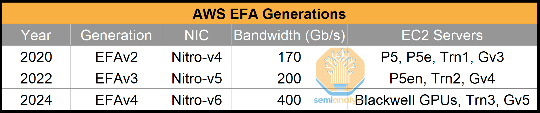
To support EFA, AWS builds custom Network Interface Cards (NICs). The table below shows each EFA Generation mapped onto specific EC2 Servers:
Contrary to our prior note on Trainium2 where we had assumed separate front-end and back-end networks, AWS, like Google, converges both traffic types onto one network. They achieve this by connecting the Nitro-v6 NICs on both the Trainium trays and the CPU trays to the same Top-of-Rack (ToR) switches.
For EFAv4 on Trainium3, there are two scale-out networking speeds available, 400G per Trainium3 with one 400G Nitro-v6 per Trainium3 chip, or one 400G Nitro-v6 shared among two Trainium3 chips, or 200G per Trainium3. Most racks produced will use the 200G per Trainium3 option, and this will be the version we will discuss and diagram below. In either case, the Nitro-v6 NIC will connect to two 200G OSFP cages.
In the 200G per Trainium3 version, each 400G Nitro-v6 NIC will support two Trainium3 chips. AWS adopts a dual Top of Rack (ToR) design where one Nitro-v6 NIC supports two 200G links each to one of two ToR switches that sit above the compute trays. A 400G Y-Cable Active Copper Cable (AEC) with a gearbox is used to convert 56G SerDes lanes at the NIC to 112G SerDes lanes at the ToR for Trainium trays while a straight AEC or Direct Active Copper (DAC) cable is used to connect the two CPU trays to the same pair of ToR switches.
Luckily for Amazon, they have an even better deal on AECs than they do on PCIe switches and retimers due to the Credo stock rebate they received. The stock rebate for Credo follows the same structure as AWS’s deal with ALAB, but the effective rebate is much larger due to the significantly higher number of warrants AWS received in this agreement and since then the huge run in the Credo share price. This means that that the value of the Credo warrants that Amazon received was more than the spend needed to vest those warrants. Credo effectively paid Amazon to take AECs!
Even though the Nvidia InfiniBand or Spectrum Ethernet reference network architectures adopt a rail-optimized clos topology to reduce the number of switch hops between GPUs, AWS prefers ToR switches for the first switch layer where possible. This reduces overall networking costs by substituting optical links with copper cables between the chip and the first switch layer. It also enables optionality should the extra uplink ports from the ToR be used for undersubscribing to the upper layers to allow for fault tolerance, virtual rails, or connections to other services. AWS claims that this tradeoff is worth it.
The default network configuration for most Neoclouds and Hyperscalers uses 400G per logical port or 800G per logical port matching the NIC bandwidth. For instance, Nvidia’s reference architecture for a 2k GPU H100 cluster will use 25.6T QM9700 InfiniBand switches featuring 64 logical ports of 400G each, matching the 400G of bandwidth per GPU offered by the CX-7 NICs. Switch math means that a 2-layer network built up with 64-port switches can only serve 2,048 GPUs at most.
The increasing adoption of higher radix networks - that is splitting links into a greater number of smaller logical ports – to increase the maximum number of GPUs on a network has shown that the approach of sticking with large default logical port sizes leaves a lot of network optimization and cost savings on the table. Our recent article on Microsoft’s Largest AI Datacenters walks through the math behind this idea.
In the Microsoft article, we also discuss how Hyperscalers are, at the behest of the largest AI Labs, now starting to deploy high radix networks. The diagram below shows one such example – OpenAI’s network at Oracle which can connect 131,072 GPUs across two layers using 100G logical ports.
AWS’s approach for AI networking has already cut to the chase and uses 100G logical ports by default. This has two main benefits:
1. AWS can build large networks with only 12.8T Switches.
If we stick with the traditional approach and use logical port sizes that match GPU NICs, 400G in many cases, we find that only using 12.8T switches would result in a network that is prohibitively small. For a two-layer network built up entirely of 12.8T switches, we can only connect 512 GPUs at most. However, if we instead use 100G logical ports, a two-layer network can reach 8,192 GPUs and a three-layer network can reach 524,288 GPUs – matching the size of today’s largest multi-building clusters.
But why build a network out of 12.8T switches? In fact, there is no such focus. AWS’s mantra is to minimize total cost of ownership and flex their procurement decisions around this north star. Metaphorically speaking, to AWS – it doesn’t matter whether the cat is black or white, as long as it catches mice. So, AWS will go with any switch option, 12.8T, 25.6T or 51.2T or 400G DR4, 800G DR8 optics, as long as it delivers the lowest cost of ownership.
2. AWS can achieve even larger scale on only two layers if we bring in 25.6T and 51.2T switches.
By the same math, AWS can achieve massive scale if they bring in 25.6T and 51.2T switches – again scale that is underestimated if we simply assume default 400G or 800G logical port sizes. In the table below, we can see how for a two-layer network, one can connect 16 times the number of GPUs when using 100G port sizes vs 400G port sizes on a 51.2T switch. For a three-layer network, this ratio expands to 64 times the number of GPUs.
The disadvantage of using 100G port sizes is that it is incredibly complex to connect – operators must ordinarily use shuffle boards and patch panels or unwieldy octopus cables to route these 100G links to the right destinations as well as a low tolerance to cabling errors. Amazon instead uses a custom optical plant, ViaPhoton, to support this cabling that minimizes the impact of this complexity.
ToR switches within each Trainium pod are split into many planes at the leaf and spine layers and are rail-optimized. All Trainium pods – which are discrete scalable units – are connected via the spine layer. In the diagram below, we hypothesize a maximum cluster size given a 3-layer network and 12.8T bandwidth switches on each plane.
Swapping in 25.6T switches instead of 12.8T switches for the leaf and spine layers means 4x more Trainium3 chips supported on the same three-layer network, with double the number of pods, and double the number of racks per pod. Moving to 51.2T switches on the leaf and spine would quadruple the number of chips on this network again.
The scale-out network can be extended to cross multiple buildings. FR optics could be used for distances of a few kilometers while ZR optics can be used for distances of up to a few hundred kilometers. Keeping with its mantra of letting NICs and the fabric manage latency that comes with longer distances, AWS will forego using deep buffer switches, directly connecting the spine layers of different buildings together.
The exact scale-across topology is not known – but the below diagram represents one topology that has been used for scale-across among various hyperscalers.
Finally – when it comes to scale-out network equipment procurement, many are receiving mixed signals about what networking architecture AWS is using for Trainium given that OpenAI’s cluster at AWS doesn’t use EFA at all. Instead, the cluster is built up using GB300s using CX-8 which runs OpenAI’s custom protocol MultiPath Reliable Connection (MRC). OpenAI might even use OCSs to connect different clusters. This has probably led to some mixed signals across the supply chain as to how exactly AWS builds up its networks and we hope this section has helped to clarify for those that are interested in understanding the core principles at work here.
Trainium3 takes a similar approach to Trainium2 and Google’s TPU and builds the chip out of a small number of large NeuronCores. This contrasts with GPU architectures like Nvidia and AMD’s, which instead uses a large number of smaller tensor cores. Large cores are typically better for GenAI workloads since they have less control overhead. As was the case for Trainium2, Trainium3 has 8 NeuronCores per package, with each NeuronCore containing the following four engines:
Tensor Engine
Vector Engine
Scalar Engine
GPSIMD
The Tensor Engine is a 128x128 BF16 Systolic Array and a 512x128 MXFP8/MXFP4 Systolic Array. The BF16 Systolic array size on Trainium3 is the same as Trn2’s BF16 array size but on FP8, it is double in size.
The systolic array that gathers its input from an SRAM buffer called “SBUF” and outputs its results into a partial sum SRAM buffer called “PSUM”. The tensor engine can loop over the K dimension of a matrix multiplication (matmul) and add up the partial sum of each result to get the complete result. The Tensor Engine / Systolic Array is where > 80% of the power and FLOPS of modern LLM workloads will be put towards. The tensor engine also supports MXFP8 4:8 and 4:16 structured sparsity offering 4x more FLOPS than their dense equivalent but we doubt this will be used by any customers.
The MXFP4/MXFP8 512x128 systolic array can also be broken down into 4x (128x128) systolic arrays such that it can push four results per cycle into the PSUM buffer. In certain GEMM shapes, there are a few optimizations that can make a 4x (128x128) systolic array performance at a better higher MFU than using 512x128 systolic array size instructions.
Typically, even for BF16/MFP8, the GEMM is fully accumulated in FP32 (in Nvidia Hopper it was only FP22), but some workloads are able tolerate slightly lower accumulation precision. For the Trainium3 Tensor Engine, there is an option to accumulate 128 elements in FP32 and then downcast it to BF16 at the end.
The Trainium3 team was able to double the MXFP8 performance in the same silicon area and power budget by only focusing on doubling MXFP8 perf and keeping BF16 perf the same along with other physical optimizations such as moving to an 3nm process, focusing on efficient floor planning and by using a custom cell library. Some other optimizations to get a higher MXFP8 FLOPS per Watt include having an updated vertical power delivery system compared to Trn2. A lot of the critical physical design work happens in house instead of outsourcing critical PD work to its vendor. To convert from master weights typically in higher precision to compute weights in lower precision, Trainium3 has hardware accelerated units in the silicon to accelerated quant/dequant of MXFP8/MXFP4.
Unfortunately, the tradeoff from only focusing on MXFP8 is that the BF16 perf did not improve. Ultra advanced L337 users like Anthropic will not need BF16 for training and they have the skillset to do MXFP8 training but the average ML trainer only knows how to do training in BF16.
Furthermore, Trainium3’s MXFP4 performance is the same as for MXFP8, but compared to AMD/Nvidia’s GPU, this is not as optimized for inference where they are able to trade off slightly lower quality for faster inferencing.
However, this won’t matter as much for memory bound workloads like inference decode because Amazon/Anthropic can just have the weights in a custom block sized 4-bit storage format while carrying out the computation in MXFP8. This technique is commonly called W4A8. For memory bound operations, using W4A8 can be considered to enable loading and storing from HBM at 2x the rate because the transfer from HBM onto the chip will happen at 4-bit instead of 8-bit and it will get dequantized on the chip before getting feed into the tensor engine.
Moreover, Trainium3 does not have support NVFP4 (block size 16, block scale format E4M3) and only has hardware support for OCP MXFP4 (block size 32, block scale format E8M0). This means that Trainium3 will require more advanced QAT/PTQ techniques compared to what is needed on Nvidia’s GPUs. The reason why E8M0 block scale is worse than E4M3 block scale is because E8M0 snaps the scale factor to the nearest 2^n. This results in more severe quantization errors. Although Trainium3 technically does support NVFP4 as storage format (or any 4 bit arbitrary storage format) and can also support online dequant to OCP MXFP8, but it does not have native hardware accelerated NVFP4 to OCP MXFP8 dequant support and must due it through an software driven approach.
Trainium3 not supporting NVFP4 makes 4-bit training much harder. Nvidia Research (and Nvidia’s marketing department) recently put out their research paper on NVFP4 training where they were able to show an experimental training recipe where 4-bit was used in the forward and backward pass. We don’t believe that frontier western labs will be adopting 4-bit floating point training for both the forward and backward pass in the next 12 months, but we do think they may pivot to 4-bit eventually when the recipe matures.
Despite this, some western frontier labs have already adopted NVFP4 for the forward pass of training but the backward pass has thus far stayed in higher precision number formats, and this appears to be working well without a very noticeable loss in quality. Some of these frontier labs that are using 4-bit floating point for the forward pass of training have already deployed these models to production with millions of active users.
The downside for AWS Trainium3 is that if 4-bit forward pass training continues to gain adoption among the most advanced users, Trainium3 may not fare well by not supporting NVFP4 (block size 16, block scale format E8M0) and by only enabling the same OCP MXFP4 (block size 32, block scale format E4M3) computation power as they do for OCP MXFP8.
The Vector Engine is designed to accelerate vector operations, which are operations where each output element depends on multiple input elements. One example of such an operation is calculating softmax in the attention layer or calculating moving averages and variance in layer/batch normalization layers.
Third is the Scalar Engine, which is designed to carry out operations with a 1:1 mapping such as element-wise operations like SeLU, or Ex.
Lastly, inside the NeuronCore, there are multiple Turing-complete GpSimd Engines that can run any arbitrary C++ code such that is easy for any C++ developer to quickly run custom operations.
The NeuronCore Scheduler can parallelize operations such that all the engines are all working at the same time. For example, in attention, the vector/scalar engine can be calculating the softmax for the current tile at the same time that the systolic array is being used to calculate the QxK^T matmul or the AxV matmul. In addition to the 1.25x faster clock speed on the Vector engine in each NeuronCore, the exponential function also runs at 4x the throughput per cycle for the Trainium3 compared to the Trn2. This is extremely important because if the exponential function (which is used in softmax) isn’t fast enough, then it will bottleneck the matmul unit operation during the overall attention operation. Blackwell also encountered this issue where the exponential unit operation wasn’t fast enough, prompting Nvidia to increase the exponential unit performance by 2x in Blackwell Ultra.
Now that we have gone through the basic building blocks of the Trainium3 microarchitecture, it’s time for a lightning round of the new/improved features that AWS architects have implemented with Trainium3:
For Trainium3 as in Trainium2, there are dozens of dedicated collective communication cores solely devoted to communicating with other chips. This is an excellent innovation as this allows for compute-communication overlapping without any contention between compute resources and communication resources.
In contrast, on Nvidia and AMD GPUs, communication operations run on the same cores (SMs) as the compute operations. Thus, the end user needs to carefully balance the ratio of SMs running communication ops with the SMs running compute ops. On GPUs, this is done using the “NCCL_MIN_CTA” env flag and is in practice involves fairly complex tuning. Due to this complexity, only the most advanced users will be doing comms/compute SMs ratio tuning.
The Trainium3 collective cores can carry out “near memory compute” (read-add-write) in one instruction to reduce the latency of collectives. Another feature of Trainium3 that reduces latency of collectives is that unlike in the case of GPUs, collectives are not required to start or end from HBM. To reduce collective latency even further, Trainium3 can transfer SBUF (software managed SRAM scratchpad) in each NeuronCore directly to the SRAM in other NeuronCores on the same package and it can also transfer directly to the SRAM on other Trainium3 packages within the scale up domain. This feature is especially useful for shifting the busBW vs message size curve to the left and to enable more performant small/medium message sizes. Furthermore, collective cores’ ability to carry out an add-write operation inside SBUF is also useful for residualAdds inside the Transformer block.
Another useful feature of Trainium3’s collective cores is auto forwarding thanks to shared SBUF memory map across the whole 144 package scale up domain. This means programmers do not have to worry about programming kernels on immediate Trainium3 chips to manually forward messages to the final Trainium3 destination chip. Due to having multiple paths from 1 chip to another chip in the time to market topology, the underlying neuron collective library must be well optimized for load balancing & congestion control especially for dynamic online all-to-all MoE dispatch & MoE combine which can’t be precomputed at compile time.
Transposes are commonly used in LLM training workloads. Trainium3, includes hardware accelerated instructions that allow transposes to effectively have “zero cost”, allowing these operations to happen in the background.
For certain workloads where the NoC/HBMs/DMA collective cores are all working at the same time, different traffic can conflict with one another other. Trainium3 introduces a new hardware feature called “traffic shaping” that provides quality of service (QoS) for different traffic classes. For instance, the compiler or end user can prioritize extremely time sensitive traffic used in Tensor Parallelism and Expert Parallelism that has many downstream dependencies, handling these before less urgent traffic like background prefetching data from the CPU or background pre-fetching weights/optimizer states (FSDP/ZeRO) for the next layer.
This feature is not user configurable on Day 0, but it will be configurable soon enough to allow kernel programmers to shape the traffic with NKI hints. In workloads with small batch size (i.e. high interactivity tok/s/user), users won’t see the benefit of this feature because the DMA/buses are not being fully utilized, but for queries that use medium/large batches of token, this feature can help reduce the latency while increasing the throughput by removing contention between traffic classes. Interestingly enough, Graviton has supported a very similar “QoS” traffic shaping feature for the past few generations now.
With Mixture of Experts (MoE) models, it is common for one to permute/shuffle tokens such that all tokens going to expert #0 are “beside” each other and all tokens going to expert #1 are “beside” each other in memory. Trainium3 introduces a feature called Tensor Dereferencing where users can dynamically index into the activation matrix even though each expert’s tokens is not strictly “beside” each other. In essence, a common issue with existing VLIW AI chip architectures is that they don’t natively support dynamism and as such, atypical workarounds are needed to determine where each expert tokens are sent to at runtime instead of compiler time as is required for modern frontier MoE models.
AWS adding this new hardware tensor dereferencing dynamism feature in Trainium3 now means that it can natively support dynamic MoE token routing in the architecture itself.
AWS is carrying out a massive course correction to their software strategy, and we believe it will be incredibly positive towards increasing the wider adoption of Trainium3. The first phase of this strategy starts with focusing on supporting PyTorch natively instead of duct-taping Trainium to PyTorch with the PyTorch/XLA project. This new PyTorch backend is meant for the non-advanced Anthropic kernel engineers of the world. In the past, users would have to rely on a lazy tensor graph capture using PyTorch/XLA instead of having a first-class eager execution mode available. Furthermore, PyTorch/XLA did not support PyTorch native distributed APIs (torch.distributed.*), nor did it support PyTorch native parallelism APIs (DTensor, FSDP2, DDP, etc). It instead relied on strange out of tree XLA SPMD APIs (torch_xla.experimental.spmd_fsdp, torch_xla.distributed.spmd, etc.). For users trying to switch to Trainium, this has led to a subpar non-native experience given that these users are accustomed to the native PyTorch CUDA.
This week, AWS announced that it will be releasing and open sourcing their native PyTorch backend that supports native PyTorch Aten op eager mode through the “PrivateUse1” TorchDispatch key. They will also support torch.compile APIs by plugging their graph compiler stack in using the torch compiler custom backend function. AWS will also support all of the native torch.distributed and parallelism APIs. There will also be DTensor, FSDP1, FSDP2, and SimpleFSDP support for eager mode. Day 0 torch.compile support will be limited to SimpleFSDP only though as it is the most compiler friendly package. However, Trainium’s torch.compile will not offer Day 0 support for capturing data dependent conditions nor will it support while loops on Day 0. This will lead to graph breaks being triggered.
AWS also claims that it will support torch native aten groupgemm MoE ops and MoE Dispatch native ops (torch.all_to_all_vdev_2d), and MoE Combine native ops (torch.all_to_all_vdev_2d_offset) on Day 0. Even AMD does not have these MoE communication ops supported yet! AWS will also offer Flex Attention support from Day 0 - this feature is needed for any ML Scientists that don’t want to just train models with vanilla causal attention.
When it comes to using Trainium3 for training workloads, AWS claims that on Day 0, their PyTorch native backend and torch.compile native graph compiler can already achieve 43% BF16 MFU on Qwen Dense variants while on Qwen MoE models it can already achieve a BF16 20-30% MFU. However, AWS claims that by using a training codebase using hand-crafted NKI (Neuron Kernal Interface, AWS’s kernel authoring language) kernels, Trainium3 can sustain a ~60% BF16 MFU for dense text models and upwards of 40% BF16 MFU on sparse MoE models like DeepSeek 670B (where only 8 out of 256 experts are active per token).
Note that the torch.compile MFU advertised above is just a Day 0 MFU and it will likely improve over time. We expect that the torch.compile performance in terms of MFU will converge towards the performance achieved when using the hand-crafted NKI kernel. With that being said, NKI kernel performance will improve as well, and clearly hand crafted NKI kernels will always be the frontier for performance especially when it comes to the latest model architectures.
End users that want to write custom kernels with NKI can do so through the use of a torch custom ops API. It is great to see that AWS is supporting the entire native PyTorch API surface from Day 0 and is allowing for break glass also through the use of custom ops.
In addition to the core in tree PyTorch native APIs, there is also work behind the scenes on integrating NKI kernel language as a codegen target for Helion. You can think of Helion as a higher-level language that can be used for writing decently performing kernels in a high level language. Users can think about Helion as a low-level Aten operator rather than as a high level Triton/NKI operator due to its similarity in that it matches much closer to the Native PyTorch Aten ops. This will allow end users that aren’t hardcode 1337 performance engineers to be able to write custom kernels too.
The new Trainium native PyTorch stack will start as an out of tree open-source GitHub-first codebase (i.e. it won’t be in the “pytorch/pytorch” repo) accessed through the use of “PrivateUse1” TorchDispatch key. However, AWS plans on moving it in tree when the software stack matures and gets approved by Meta. Although on paper, PyTorch is now controlled by the non-profit Linux Foundation, because most of the maintainers and contributors to PyTorch are still at Meta, Meta still calls the shots on which chips get approved to be moved in tree.
Fortunately for Trainium, AWS already has a lot of clout with the Meta PyTorch team since most of the existing open source PyTorch CI for CPUs and Nvidia GPUs runs on AWS infrastructure. In fact, AWS contributes most of this cloud infra to Meta PyTorch for free, building up a lot of good will and rapport. The upshot is that once the native Trainium PyTorch stack is mature, AWS should have no trouble convincing Meta to allow in-tree (aten/src/Aten/native/neuron).
We attended and observed the PyTorch Technical Advisory Council, and there has been a recent proposal submitted called “PyTorch Compute Platform Quality Levels” which defines 3 levels of stability:
Stable
Unstable
Engineering
To get upstreamed into PyTorch in-tree and get added to pytorch.org documentation and to have download links set up on pytorch.org’s get started page, a package must score above a certain point threshold on this quality level scorecard. We believe that the Trainium PyTorch native stack will be able to hit this threshold at least for the testing requirements by Q1 2026 in their out of tree repo, but moving to an in tree repo will still take a some time. We estimate that it will be around end of 2026 for when it moves in tree but there isn’t yet an concrete timeline yet. We will discuss the “PyTorch Compute Platform Quality Levels” RFC along with other major developments in the PyTorch ecosystem in our upcoming State of PyTorch article.
Trainium’s native PyTorch will eventually have open-source CI to support an open-source GitHub-first approach. SemiAnalysis has been the PyTorch CI Karen when it comes to ensuring that all the current 600+ unit tests/integration tests/model accuracy tests that are missing from AMD’s ROCm will get addressed.
SemiAnalysis has also been the PyTorch CI Karen for Nvidia to ensure that they contribute their fair share of CI machines to the PyTorch Foundation and do not just have AWS/Meta foot the bill for Nvidia GPU CI. We convinced Nvidia to directly contribute 48 B200s to PyTorch Foundation back in June 2025 and also convinced Nvidia to start financially contributing to PyTorch Foundation CI. SemiAnalysis will soon be the PyTorch CI Karen for Intel GPGPU as well, but will not be taking this role for the Intel Gaudi software stack as it is at Gaudi is end of life. Once Trainium PyTorch Native gets open sourced, we will 110% be the PyTorch CI Karen for Trainium as well.
On Day 0, the Trainium PyTorch Native stack will support TorchTitan. But support for other PyTorch ecosystem libraries like Torchcomm, TorchMonarch, TorchForge, TorchAO for low precision training, will have to wait until around Q2 2026.
When it comes to inference, Trainium will support a native vLLM v1 experience on Day 0 instead of the current patchwork Trainium XLA vLLM experience. We believe that vLLM Trainium will potentially be upstreamable by mid 2026 and will be a much cleaner integration than the TPU<>vLLM integration, which literally translates the vLLM PyTorch code into JAX.
AWS has made the interesting choice to standardize on using Nvidia’s NIXL KV Transfer library for KV cache transfer between prefill instances and decode instances. They have made this decision so that they can move KV cache between Trn2/Trainium3/H100/H200/B300/etc if these systems are on the same fabric.
This will allow users to mix and match across different inference systems for prefill instances and decode instances with the goal of optimizing the AZ/Datacenter throughput per second (normalized by TCO, of course) subject to end-to-end latency and interactivity (tok/s/user) objectives.
For example, one can use a B200 for prefill and transfer KV cache over using NIXL (over EFA) to the Trainium3 NL72x2 Switched for decoding. Interestingly, Nvidia has accepted AWS PR’s for Nvidia GPUs EFA into the upstream NIXL. Merging Trainium code into Nvidia upstream NIXL, however, is still a work in progress as it is still pending for Nvidia to be convinced to accept it and so it currently sits in an AWS engineer’s fork.
Rounding out and summarizing Amazon’s open sourcing roadmap, AWS will open source all the PyTorch stack as well as NKI communication, GEMM, attention, and kernel libraries (among many others) in the first phase of the open-source push. For the second phase of the open sourcing push, AWS will be open sourcing their XLA graph compiler and the JAX software stack.
On Day 0, Trn2/3 software will only support each logical device mapping onto either 1 or 2 physical neuron cores, meaning that there will be 4 logical devices per Trainium package. What this means is that each logical device exposed to the user & ML application only gets 36GB of HBM instead of the full 144GB. There are nuances and important pros and cons with this to unpack and it’s unfortunate that there is no Day 0 option for each logical device to map onto the entire package (8 NeuronCores), with users instead having to wait until mid-2026. We strongly believe that mapping the entire package (8 NeuronCores) onto 1 logical device is needed for wider ML research adoption of the Trainium stack.
With LNC=1 or LNC=2, because each NeuronCore is fully exposed to the end user programmer, advanced L337 users like Anthropic’s elite performance engineers can fully control reading from HBM and can directly manage data movements between the 8 Neuron cores on the chip thus reducing unnecessary data movement. elite kernel programmers love this feature and will continue to use it. LNC=1 or LNC=2 will always have better performance than LNC=8.
On the other hand, the disadvantage of LNC=1 or LNC=2 is that since each logical device only sees 36GB of memory, research scientists and the “average” end ML researcher doing small scale ablations and experiments will need to start worrying about parallelism at a 4x smaller models/batch size as opposed to if there was an LNC=8 option available that would expose 1 logical device being the full 8 physical neuron cores and 144GB of memory along with it.
On other merchant silicon architectures, ML research scientists only need to start worrying about model parallelism beyond simple data parallelism strategies when sizes exceed 80GB when working with an H100 (i.e. 2.2x higher than Trainium3 Day 0 LHC=1 or LHC=2 support). The headroom is even greater with the 288GB of memory on the GB300, an amount 8x higher than Trainium3’s Day 0 logical device mapping.
One might argue that any researcher worth their salt can figure out FSDP – admittedly a true statement – but it is also true that introducing FSDP adds another layer of indirection which is not desirable when working on small scale experiments where researchers typically want to minimize the number of layers of indirection.
In a perfect world, the PyTorch FSDP API would be flawless and bug-free but as everyone knows, this is only the case in a fantasy world, and in the real world there are usually specific errors that get introduced when using FSDP. Why do you think there multiple generations of FSDP APIs? FSDP1/FSDP2/SimpleFSDP…
For what is it worth, SimpleFSDP/DTensor is heading in the correct direction to offer a clean FSDP API.
On the MI250X, showing PyTorch each of the 2 chiplets on the package as separate logical devices used to be the only option. On MI300/MI325/MI355, AMD recognized that this led to a poor user experience and changed this such that the default option is now 1 full package mapped to 1 logical device, though they still kept the option to expose each chiplet as a separate logical device. Comparing this to the LNC=1 or LNC=2 options for the Trainium3 as used by Anthropic, it is important to note that in practice nobody who currently uses the MI355X in volume will actually use the option to map 1 logical devices to 1 XCD mapping.
The reason AWS hasn’t implemented LNC=8 yet it is because building a compiler that maps 1 logical device to 8 physical cores all while minimizing unnecessary communication between the cores is a time-consuming problem and it unfortunately is not high on Anthropic/Bedrock’s priority list. So the end result is Trainium3 will “crawl before it walks” and come to market with LNC=1 or LNC=2, which is what their largest existing customer Anthropic uses anyway, before attempting the task of implementing LNC=8.
Trainium3 will hardly be an outlier in this regard. In fact, Google’s TPU only supported an LNC=1 option from the 1st to the 3rd TPU generations. For TPUv3, each package had 2 logical devices, and it was only by early 2022 that support for mapping each logical device onto the entire package came as the TPUv4 came to market. The compiler for this mapping in the Google TPU stack is called “MegaCore”.
Google now supports MegaCore for the TPUv4/v5p/v6e, and it has led to a better user experience. On the TPUv7e, Google has gone back to only offering “LNC=1” i.e. although each package has 2 physical cores, each logical device will only map to 1 of these physical cores. While this will be great for performance, we still recommend that Google support the use of “MegaCore” for TPUv7 as well.
One of the areas that Trainium’s software is already better than that of Nvidia is the Neuron Explorer performance analysis suite. This suite has been available as a web application (similar to Chrome Trace/Perfetto/Tensorboard), but now it is also available through a VSCode integration.
Trainium’s low level profiler is loved by all the 1337 performance engineers at Anthropic with Anthropic’s head of performance publicly saying that performance analysis on Trainium is way better than performance analysis on Nvidia GPUs (and obviously better than on AMD GPUs too).
Neuron Explorer shows the metrics that performance engineers care about. It has a quick high level summary page for reporting the average athematic intensity and MFU/HFU in addition to displaying DMA/HBM metrics. It also shows the activity percentage of all 4 engines per NeuronCore.
Like Nsight Compute, Neuron Explorer can give users automated recommendations which Anthropic/AWS engineers claim are even better than those provided by Nvidia’s performance analysis tools.
When it comes to collectives, Neuron Explorer features an overview showing collective operation duration distributions grouped by the collective operation (i.e. allreduce, allgather, etc) and grouped by message sizes. Performance engineers can analyze this distribution chart and aim to minimize the duration distribution spread by optimizing traffic patterns so as to reduce contention.
The Neuron Explorer also includes a timeline of the utilization of all major units over time such that engineers can turn performance optimization into a game of Factorio. Users can investigate where the bottleneck is by simply clicking into the NKI kernel source code and looking at how to remove that bottleneck.
A few months ago, we laid out our Amazon’s AI Resurgence thesis – which has already proven accurate after Q3’25 earnings. By estimating a precise start of construction and ultimate full capacity for every single Project Rainier building, we were able to predict a growth acceleration at AWS. While many others are struggling with delays, AWS’ execution has been impressive. We expect continued growth acceleration driven by this buildout.
However, these datacenters barely represent even the first phases of the multi-gigawatt Project Rainier buildout. For Trainium3, AWS has various campuses well under construction that are equally as impressive. Below, we show an example of a new major AWS campus dedicated to Project Rainier which will eventually scale up to 1GW. This new campus is located near a metro area and will be connected to an adjacent 1GW site which has also broken ground. This capacity is incremental to the expansion of existing sites like Indiana. Our Datacenter Industry Model forecasts precise quarterly MWs and start of datacenter operations for each building.
Another remarkable aspect of Amazon’s AI ASIC roadmap is the relative absence of liquid cooling, from silicon to datacenter. This is at odds with others that underwent full design changes – such as Meta’s drastic pivot we covered last year.
Amazon’s datacenter design has barely changed over the years. We show below the design of a 2021 campus in Virginia, comparing this campus to the flagship Project Rainier AI cluster in Indiana, we see that the building designs are nearly identical!
While there are some minor changes, the cooling system remains largely the same. A year ago, our deep dive on Datacenter Cooling Systems explained how AWS largely relies on external air as a means to cool their datacenters.
A simple look at satellite imagery of an AWS facility will reveal the absence of any fluid cooling loop or piping system. Said differently – AWS datacenters have been hyper-optimized for air cooling for many years, and the Cloud giant isn’t changing course in the GenAI era or deviating from its mantra of delivering lowest total cost of ownership and fastest time to market.
Many interpret this as a sign that Amazon is late and misunderstands AI, but we believe it is a conscious and sensible decision.
From a time-to-market perspective, AWS benefits enormously by building an extremely standardized and proven design, thereby avoiding any delays related to a full redesign. It has worked out nicely for the first phases of Project Rainier, to Anthropic’s benefit.
Fungibility is another advantage. AWS can remain agnostic and avoids being captive to any cooling architecture as it can easily place both CPUs and Trainium3s in any datacenter. While liquid-cooled chips like GB200 are more challenging to deploy when using liquid to liquid cooling, a sidecar can be used to sidestep this challenge. TCO might be an issue, but the operational flexibility of deploying workloads anywhere is extremely valuable and is not to be underestimated.
Total Cost of Ownership vs operational flexibility is indeed a contentious topic. In our view, many in the industry are not building fully liquid-optimized datacenters. As such, we’ve seen CapEx/MW go up dramatically. Counter-intuitively, an air-optimized facility can even be more energy-efficient. While many think DLC reduces PUE, the reality is often different. Many designs are adopting a central water pipe for both the air and liquid loop, as opposed to two dedicated circuits. A central pipe typically operates at 25-30C inlet (if not below 25C), meaning that the chilled water plant requires a chiller for peak summer days. The need for a chiller means: (1) CapEx is increased, relative to an air-optimized facility with evaporative air intake (such as AWS’ typical datacenters). (2) IT MWs are reduced, as peak PUE goes from ~1.2x to ~1.5x due to peak scenario days. (3) OpEx is typically higher, as an air-optimized facility with high inlet temperature runs all year without chillers, removing the need for mechanical cooling and extra energy.
We explained all of these concepts in detail last year in our deep dive on Cooling Systems. Deploying a true DLC-optimized datacenter remains a huge challenge. Many operators fear they might lose “fungibility” if they over-optimize, leading them to pick designs that increase both Capex and Opex relative to traditional air-optimized facilities.
Next, we will talk about the total cost of ownership and how the performance per TCO of Trainium3 compares with Nvidia and Trn2. Subscribers of our AI TCO Model and our AI Hardware Bill of Materials (BoM) Model can see granular details on quantities, ASPs and total system cost.